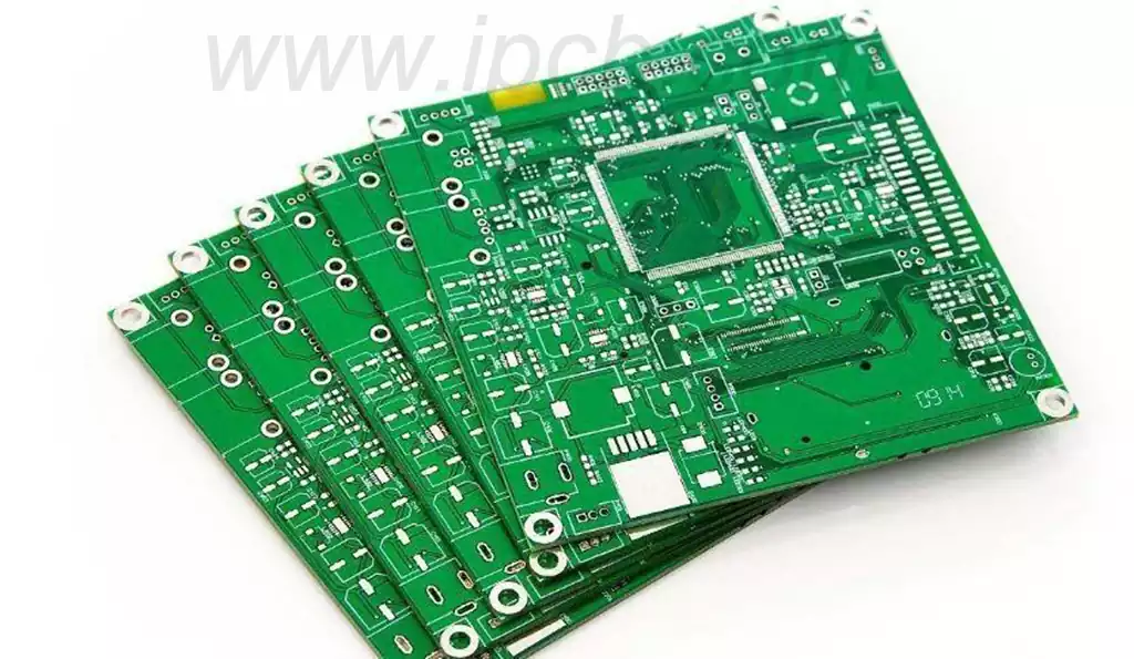
In the field of electronic circuit design, the PCB (printed circuit board) serves as the substrate for electronic components, with its performance directly impacting the quality and reliability of the entire electronic product. PCB laminate design, as a critical component of PCB design, functions like the foundational structure of a precision-engineered building, playing a decisive role in circuit performance. It not only concerns the manifestation of signal integrity, power integrity, electromagnetic compatibility, and thermal performance, but is also the core factor determining whether a product can successfully pass EMC testing.
PCB laminate design plays a crucial role in circuit performance, directly impacting signal integrity, power integrity, electromagnetic compatibility, and thermal characteristics. It is a core factor determining whether a product can successfully pass EMC testing. The lamination design of multilayer PCBs fundamentally involves the scientific and rational arrangement of circuit board layers. This seemingly straightforward arrangement operation actually requires profound professional knowledge and extensive practical experience, directly impacting numerous critical performance metrics such as signal integrity, power integrity, electromagnetic compatibility, and thermal performance.
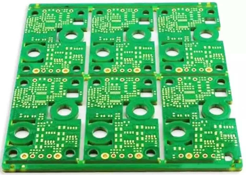
When undertaking lamination design work, many engineers tend to fall into certain misconceptions. They often mistakenly believe that more layers equate to better design outcomes, yet this is not necessarily the case. The number of layers must be determined in close alignment with actual application requirements. Excessive or insufficient layers can both trigger a series of issues, preventing the achievement of the intended design results. Therefore, the selection of layers must be precisely determined based on practical needs, avoiding arbitrary increases or decreases.
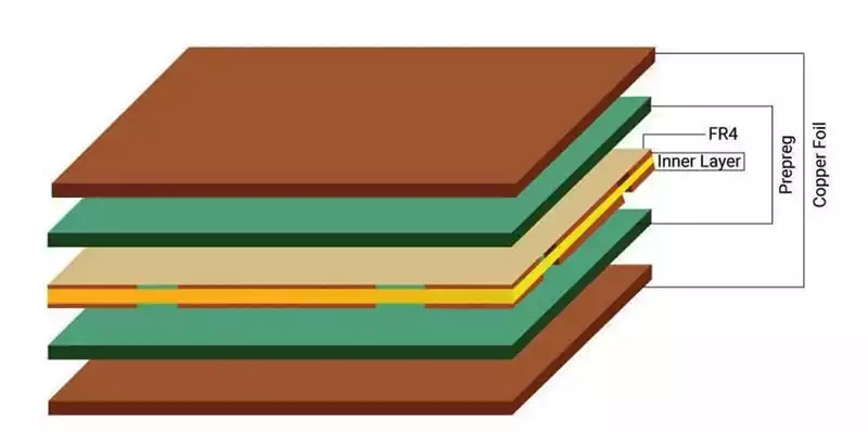
Beyond the number of layers, dielectric thickness is another critical parameter requiring close attention during the design process. The thickness of the dielectric directly influences the coupling effect between the signal layer and the ground plane. While ensuring manufacturability, the dielectric thickness should be minimised wherever feasible to enhance coupling and effectively reduce electromagnetic interference (EMI). However, an excessive pursuit of thin dielectrics must be avoided, as this can significantly increase manufacturing complexity and cost. When selecting dielectric materials, a comprehensive evaluation of all factors is essential to strike a balance between performance and cost. Whilst advanced materials like Rogers offer exceptional performance, they are typically costly and demand sophisticated manufacturing processes. For most standard applications, conventional materials such as FR-4 adequately fulfil fundamental requirements. Advanced materials warrant consideration only in specialised scenarios involving extremely high operating frequencies or precise impedance control.
Optimised PCB Laminate Layout Schemes
For common four-layer boards, the recommended stack-up configuration is:
Signal Layer – Ground Layer – power plane – signal layer” configuration. This design offers significant advantages during upgrades of legacy products, as simple adjustments to the layer stack can substantially reduce radiated interference. This structure provides the outer signal layers with a complete reference plane, ensuring the intermediate ground and power planes form low-impedance current loops.
When designing 6-layer boards, the recommended configuration is “signal layer – ground plane – signal layer – Signal Layer – Power Layer – Ground Layer” configuration. This layout not only effectively mitigates crosstalk between signals but also further enhances signal integrity. In this design, the top and bottom signal layers utilise the second layer’s ground plane as their reference plane, while the intermediate signal layers employ both the ground and power planes as references, thereby providing a more stable environment for signal transmission.
Common Design Issues and Mitigation Strategies
Caution must be exercised regarding via usage. Whilst unavoidable in design, vias can become sources of signal reflection and electromagnetic radiation. Consequently, meticulous planning of via placement and spacing is essential during the design phase to prevent unnecessary interference arising from improper via layout.
A well-considered pcb laminate design does not inherently equate to high costs. By comprehensively evaluating the criticality of different signals and manufacturing constraints, it is entirely possible to identify both economical and efficient design solutions. For instance, non-critical signals may benefit from relaxed layer spacing requirements. In specific areas, tailored laminate strategies can be employed based on actual needs to achieve either performance optimisation or cost reduction.
PCB laminate design is a complex process involving multiple factors and requiring comprehensive trade-offs. From avoiding common misconceptions to rationally selecting layer count, dielectric thickness, and materials; from implementing optimised stack-up layouts for different layer configurations to judicious use of vias and effective cost control – each stage is intrinsically linked, collectively influencing circuit performance and product quality. Only by thoroughly mastering these principles and executing scientifically sound design can one produce high-performance, cost-controlled PCBs that provide a robust foundation for the stable operation of electronic products.