In the field of electronics, the design and development of printed circuit board assemblies (PCBAs) are critical to the functionality and reliability of electronic devices. PCBA design is a complex and multifaceted process that requires careful planning and execution to ensure that the final product performs as intended. This guide offers an in-depth look at PCBA design, highlighting best practices, common challenges, and strategies for optimizing the design process.
Understanding PCBA Design
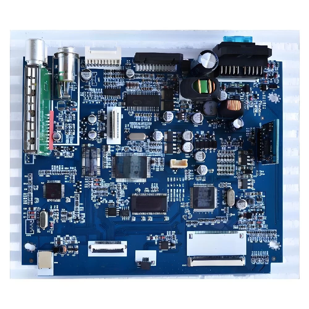
PCBA design involves designing and developing a printed circuit board assembly, which includes both the PCB and the electronic components mounted on it. This process encompasses several stages, each with its own set of considerations that affect the overall quality and performance of the PCBA.
Schematic Capture
The first step in PCBA design is schematic capture, where the electrical circuit of the device is represented using symbols and connections. This stage involves creating a detailed schematic diagram that shows how components are interconnected and how they function within the circuit. A well-designed schematic serves as the blueprint for the subsequent PCB layout and ensures that the circuit operates correctly.
Key considerations during schematic capture include selecting appropriate components, defining component values, and ensuring that all connections are accurate. Utilizing advanced schematic capture tools can streamline this process and help identify potential issues early on. Additionally, ensure that the schematic adheres to standard practices and conventions to facilitate easier understanding and modifications in future stages.
PCB Layout Design
Once the schematic is completed, the next phase in PCBA design is PCB layout design. This stage involves translating the schematic diagram into a physical layout that defines component placement and trace routing on the PCB. The goal is to create a layout that satisfies electrical, mechanical, and thermal requirements while ensuring that the board is manufacturable.
Important factors to consider during PCB layout design include:
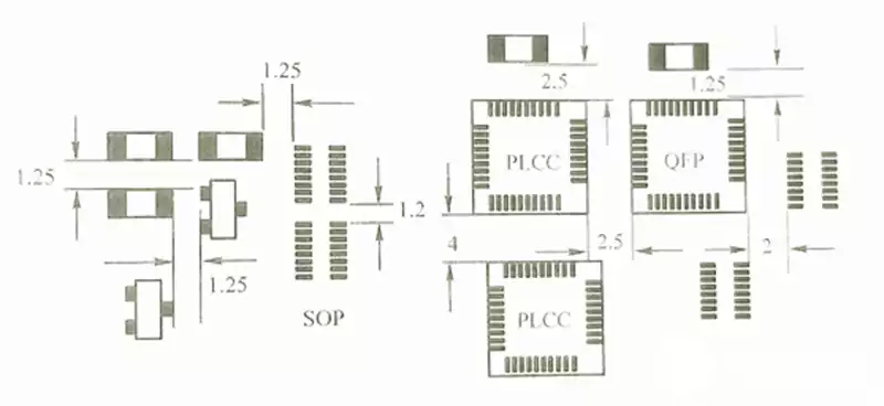
- Component Placement: Proper component placement is crucial for maintaining signal integrity and minimizing interference. Components should be arranged in a logical sequence that follows the signal flow and minimizes the length of critical traces. Additionally, consider thermal management by placing heat-sensitive components away from heat sources and using appropriate thermal vias or heat sinks.
- Trace Routing: Routing electrical traces involves connecting components according to the schematic while optimizing trace lengths and minimizing signal degradation. Pay careful attention to trace width and spacing to meet electrical performance standards and manufacturing constraints. Employing techniques like differential pair routing for high-speed signals can enhance performance and reduce noise.
- Grounding and Power Distribution: Effective grounding and power distribution are vital for minimizing noise and ensuring stable operation. Implement ground planes and power planes to provide a low-impedance path for current and reduce electromagnetic interference. Properly designed grounding helps in reducing ground loop issues and enhancing overall circuit reliability.
- Design for Manufacturability (DFM): Ensuring that the PCB layout adheres to manufacturing constraints, such as minimum trace width and spacing, is essential for avoiding production issues. DFM practices help prevent design errors that could lead to costly rework or yield loss during manufacturing. Collaborating closely with PCB manufacturers during the design phase can help address potential manufacturability issues early.
- Mechanical Considerations: During PCB layout design, mechanical constraints such as board size, mounting hole placement, and connector locations must be considered. Proper alignment and mounting provisions are essential to ensure that the PCB fits within the intended enclosure and aligns with other mechanical components.
Component Selection and Placement
Selecting the right components for your PCBA design is crucial for achieving the desired functionality and performance. Consider factors such as component specifications, availability, and cost. Ensure that the components chosen are compatible with the PCB layout and can be reliably soldered during assembly.
When placing components, consider the following:
- Accessibility: Components should be placed in a way that facilitates easy soldering and inspection. Avoid positioning components in hard-to-reach areas or those that require complex soldering techniques. This not only simplifies the assembly process but also improves the overall reliability of the PCBA.
- Thermal Management: Components that generate significant heat should be strategically placed to prevent overheating of other sensitive components. Effective thermal management can be achieved through the use of thermal vias, heat sinks, and proper spacing. This helps in maintaining the longevity and performance of the components.
- Signal Integrity: For high-speed or analog circuits, ensure that critical components are placed to minimize signal degradation and interference. Pay attention to the placement of decoupling capacitors, signal conditioning components, and any required shielding to maintain signal integrity.
- Mechanical Mounting: Consider the mechanical aspects of component placement, such as the need for secure mounting and alignment with external connectors or mounting holes. Proper mechanical placement ensures that the components are well-supported and aligned with the intended product design.
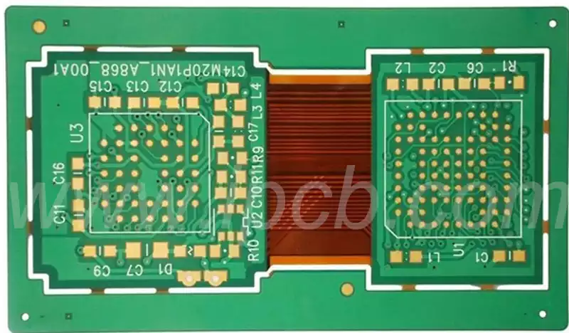
PCB Fabrication and Assembly
After completing the PCBA design, the next phase involves PCB fabrication and assembly. This process includes manufacturing the PCB based on design files and assembling the electronic components onto the board. The quality of the final PCBA depends heavily on the accuracy and precision of both fabrication and assembly processes.
Key considerations for PCB fabrication and assembly include:
- Fabrication Quality: Verify that the PCB manufacturer adheres to the design specifications and quality standards. Inspect the PCB for any defects, such as misalignment or improper etching, that could impact performance. Ensure that the PCB’s physical characteristics meet the design requirements, including layer count, thickness, and copper weight.
- Assembly Process: Choose an assembly process that aligns with the design requirements, whether it’s surface-mount technology (SMT) or through-hole technology. Ensure that the soldering process is reliable and that components are correctly placed and soldered. Evaluate the assembly partner’s capabilities and experience to ensure they can meet your design specifications.
- Testing and Verification: Conduct thorough testing and verification of the assembled PCBA to identify any issues before final deployment. Utilize functional testing, electrical testing, and visual inspection methods to ensure the quality and functionality of the PCBA. Early testing can help detect problems that might not be apparent during the initial stages of assembly.
- Quality Assurance: Implement quality assurance practices throughout the fabrication and assembly processes. This includes performing regular inspections, adhering to quality control standards, and addressing any issues promptly to ensure the final PCBA meets all performance and reliability requirements.
Common Challenges in PCBA Design
PCBA design can present several challenges that impact the quality and performance of the final product. Some common challenges include:
- Signal Integrity Issues: High-speed or analog circuits are vulnerable to signal integrity problems such as crosstalk, noise, and signal degradation. Employing proper PCB layout techniques, such as controlled impedance traces and proper grounding, can help mitigate these issues and improve overall performance. Additionally, consider signal reflection and transmission line effects when designing high-speed circuits.
- Thermal Management: Adequate thermal management is crucial for ensuring the reliability and longevity of electronic components. Poor heat dissipation can lead to overheating and component failure. Implementing effective thermal management strategies, such as thermal vias, heat sinks, and appropriate component placement, can address these challenges and enhance the PCBA’s reliability.
- Component Placement Constraints: Limited space on the PCB can make component placement challenging, especially for complex designs with many components. Efficient layout and placement techniques, such as using smaller components or optimizing component placement, can help make the best use of available space and improve the design’s overall effectiveness. Consider the impact of component placement on assembly automation and manual soldering.
- Manufacturing Constraints: Adhering to manufacturing constraints, such as minimum trace width and spacing, is essential for successful production. Design for manufacturability (DFM) practices can help address these constraints and reduce the risk of production issues. Collaborating with manufacturers early in the design process can also help identify and address potential manufacturability issues.
- Cost Management: Balancing performance, reliability, and cost is a key consideration in PCBA design. Choosing cost-effective components and optimizing the design for manufacturability can help manage production costs. Additionally, consider the long-term cost implications of component choices, such as availability and potential obsolescence. Evaluate cost-effective manufacturing processes and materials that align with your design goals.
Best Practices for Optimizing PCBA Design
To achieve a high-quality PCBA design, consider implementing the following best practices:
- Early Design Review: Conduct design reviews early in the development process to identify potential issues and make necessary adjustments. Early reviews can help prevent costly design changes later in the process and ensure that the design meets all performance and manufacturability requirements. Engage with cross-functional teams, including engineering and manufacturing, to gain diverse perspectives on design challenges.
- Use Design Tools: Leverage advanced PCB design tools and software to streamline the design process and improve accuracy. These tools can assist with schematic capture, PCB layout, and design rule checking, helping to identify potential issues and ensure compliance with design standards. Stay updated on the latest tools and technologies to enhance your design capabilities.
- Follow Industry Standards: Adhere to industry standards and best practices for PCB design to ensure compatibility and reliability. Standards such as IPC-2221 and IPC-7351 provide guidelines for design and manufacturing, helping to maintain consistency and quality throughout the design process. Familiarize yourself with relevant standards and incorporate them into your design practices.
- Prototype Testing: Build and test prototypes before finalizing the design to validate functionality and performance. Prototype testing can help identify and address any issues before mass production, reducing the risk of costly design changes and ensuring a higher level of quality in the final product. Use prototypes to evaluate real-world performance and make necessary adjustments.
- Collaborate with Manufacturers: Work closely with PCB manufacturers and assembly partners to ensure that the design meets manufacturing constraints and quality standards. Effective communication and collaboration can help prevent misunderstandings and improve the overall quality of the PCBA. Provide detailed design documentation and specifications to facilitate a smooth manufacturing process.
- Implement Design Iterations: Be prepared to iterate on the design based on feedback from testing, prototyping, and manufacturing. Design iterations allow for continuous improvement and refinement of the PCBA, leading to a more reliable and high-performing final product. Incorporate feedback from all stakeholders to address any issues and enhance the design.
Conclusion
PCBA design is a critical aspect of developing reliable and high-performance electronic devices. By understanding the key stages of PCBA design, including schematic capture, PCB layout, and component placement, manufacturers can create effective designs that meet performance, reliability, and manufacturability requirements. Addressing common challenges and following best practices can help optimize the design process and ensure the successful production of high-quality PCBAs.
With careful planning, attention to detail, and adherence to industry standards, PCBA design can significantly impact the success of electronic products and contribute to the development of innovative and reliable technologies. As technology continues to advance, staying informed about the latest design practices and trends will be essential for maintaining a competitive edge in the electronics industry.
By incorporating these best practices and addressing potential challenges, designers can create PCBAs that not only meet but exceed performance expectations, ensuring that electronic devices function optimally and reliably in real-world applications.