Although the field of radio frequency (RF) circuit board design is still full of unknowns, there are a number of guiding principles that can be followed. However, the main challenge encountered in the actual design process is how to make reasonable compromises when these principles cannot be fully followed due to various constraints.
A few key points in RF circuit board design
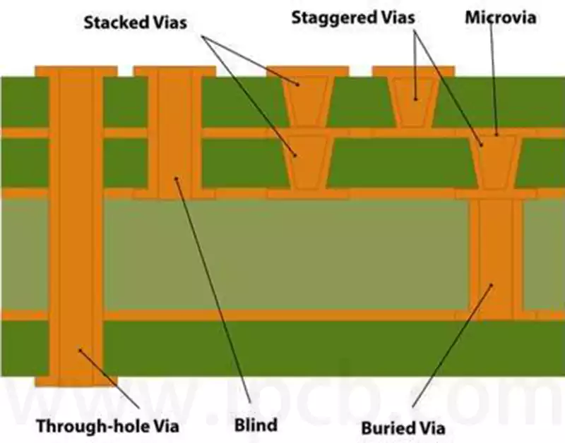
1.Classification of microvias
The use of microvias is essential for connecting the various circuits on a circuit board under ideal conditions to avoid electromagnetic interference. Microvias typically range in diameter from 0.05 to 0.20 mm and can be further classified into the following three types: blind via, buried via and through via.
Blind vias with a certain depth are created on the top and bottom surfaces of the board in order to connect the surface circuits to the internal circuits on the bottom layer of the printed circuit board. Typically, the depth of these blind vias does not exceed a specific ratio (relative to the aperture diameter).
Buried vias are connection holes that are located only in the inner layer of the printed circuit board and do not extend to the surface of the board. The inner layers of the board may contain both blind and buried vias as mentioned above. Through-holes are formed prior to lamination, and multiple inner layers may overlap each other during this process.
The third type is the through-hole, which runs through the entire board and can be used both to realise internal connections and as fixed mounting holes for components.
2.Applying Partitioning Strategies
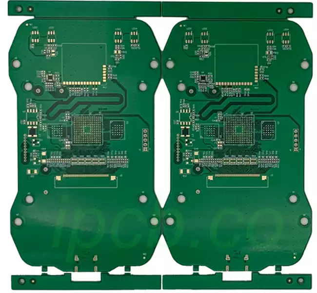
During the RF circuit board design, the low noise amplifier (LNA) should be separated from the high power RF amplifier (HPA) as much as possible in order to optimise performance. In short, the circuits responsible for low noise reception should be isolated from the circuits responsible for high power RF transmission. This requirement is relatively easy to fulfil if there is sufficient space on the PCB. However, in the case of dense components, it is indeed challenging to realise this as the PCB manufacturing area is often very limited. One solution is to place the two types of circuits on opposite sides of the PCB, or to use a staggered layout to avoid them operating simultaneously. In high power systems, it is sometimes necessary to introduce RF buffers and voltage controlled oscillators (VCOs).
Design partitioning can be subdivided into two categories: physical partitioning and electrical partitioning. Electrical partitioning can be further subdivided into power distribution partitioning, RF routing partitioning, sensitive circuit and signal partitioning, and grounding partitioning. Physical partitioning is mainly focused on solving practical problems such as component layout, direction and shielding.
- Entity Separation Strategy
The success of an RF circuit board design depends heavily on the layout of the components. An effective way to do this is to first locate the components on the RF path and then reorient them to shorten the transmission path of the RF signal. At the same time, high power circuits and low noise circuits should be located away from the RF inputs and outputs respectively.
According to the best board stacking scheme, the main ground layer should be set at the second layer below the surface layer, and the RF circuits should be placed on the surface layer as far as possible. On the RF channels, the vias should be as small as possible to reduce path inductance, virtual connection points on the main ground layer, and the risk of RF energy leakage to adjacent layers of the stacked board.
Since diplexers, mixers, and IF amplifiers typically contain a large number of interfering RF/IF signals, care must be taken to minimise these interferences. In terms of physical layout, linear circuits such as multistage amplifiers are usually sufficient to separate the various RF regions. To minimise interference in the ground plane, RF and IF circuits should avoid crossing as much as possible. Component layout usually takes up most of the time when designing a mobile phone PCB, as the correct RF path is critical to the performance of the entire PCB.
Low noise amplifier circuits and high power amplifiers can usually be arranged on opposite sides of the handset PCB prototyping board, with subsequent connection to the other end of the baseband processor via a duplexer located on one side and an RF antenna on the same side. A number of measures must be taken to prevent RF energy from being conducted from one side of the board to the other through vias. One common practice is to use blind vias on both sides. These blind vias should be placed on both sides of the PCB away from RF interference to minimise the possible adverse effects of the vias.
Core elements of RF circuit board design:
Material selection considerations:
Select low-loss dielectrics such as PTFE (polytetrafluoroethylene) or high-performance ceramic fillers.
Selection of boards with appropriate dielectric constants and low transmission loss characteristics.
Impedance matching:
Ensure that the characteristic impedance of the transmission line remains constant, with a standard value of 50 ohms.
Use impedance control tools for precise design.
Optimised laminate construction:
Adopt multi-layer board architecture to build efficient ground and power planes.
Properly plan the layout of signal, ground and power layers to reduce crosstalk and noise.
Component layout strategy:
Locate sensitive components (e.g., LNAs) away from high radiation sources (e.g., power amplifiers).
Reduce the length of the RF path to reduce loss and interference.
Alignment Layout Principles:
Avoid sharp or right-angled alignments and use rounded or 45-degree angles for smooth transitions.
Keep the width of the transmission line constant and avoid sudden changes in width.
Grounding and shielding measures:
Provide a continuous ground plane to reduce ground loop impedance.
Introduce metal shielding shells to isolate sensitive circuits from high radiation sources.
Over-hole Design Points:
Minimise the number of vias to reduce signal loss.
Design as blind or buried vias to reduce the impact on the signal layer.
Power and Ground Planning:
Provide pure power for RF circuits, use decoupling capacitors and proper power line width.
Avoid long power lines to reduce noise coupling.
Thermal Management Solutions:
Consider the heat dissipation needs of RF components and design efficient heat dissipation channels.
Signal Integrity Guarantee:
Perform signal integrity analysis with the help of simulation tools to ensure that there are no reflections or distortions in the signal.
Electromagnetic compatibility (EMC) design:
Incorporate EMC requirements in the design phase to reduce electromagnetic interference and improve system immunity.
Test and Verification Process:
Implementing test and verification during the design phase, including prototype testing and performance verification.
RF circuit board design is a complex and challenging process, in the actual design, the designer needs to consider a variety of factors, weigh the pros and cons, in order to find the best design solution. At the same time, with the continuous progress of technology and changing needs, RF circuit board design will continue to evolve to adapt to new challenges and opportunities. Therefore, designers need to maintain a learning and innovative attitude to continuously improve their professional skills and knowledge to meet future challenges.