Laser engraving pcb board is the process of processing and engraving circuit boards using laser technology. Laser engraving pcb board mainly uses the laser’s high energy density and precise control ability, through the laser beam directly on the circuit board for cutting, engraving and marking operations.
Basic Principle of Laser engraving pcb board Marking
The basic principle of laser engraving pcb board is to use a high energy density laser beam to irradiate the surface of the circuit board, through the thermal effect of the material melting, vaporisation or ablation, so as to achieve precise cutting and engraving. The high energy density and fine beam of the laser beam can achieve micron-level processing accuracy, which is suitable for high precision circuit board manufacturing and repair.
The process of laser engraving pcb board can be divided into five major steps: design preparation, graphic transfer, laser etching, chemical etching and post-processing.
Design preparation:
Use professional software (such as Eagle, Protel, Altium Designer, etc.) to design the circuit board graphics, to ensure that the wiring is reasonable, to avoid excessively long or dense wires. After the design is completed, export the graphics to a file format suitable for laser engraving (such as BMP, AI, PLT, etc.).
Prepare the copper cladding board and select the appropriate copper layer thickness and board size according to the design requirements.
Graphics transfer:
Print the designed circuit board graphics onto transfer paper (need to be set to black and white mode), or directly import the graphics file into the laser engraver control system.
If the traditional transfer method is used, the printed graphic can be covered on the copper-clad board, and the graphic can be transferred to the surface of the copper layer through thermal transfer or photosensitive plate exposure. If a laser engraver is used for direct engraving, this step is not required and the process proceeds directly to the next step.
Laser Etching:
Fix the copper-clad plate on the laser engraving machine table and adjust the laser head to a suitable position.
According to the thickness of the copper layer, material properties and design requirements, set the laser engraving parameters, including laser power, engraving speed, frequency, depth of focus and so on.
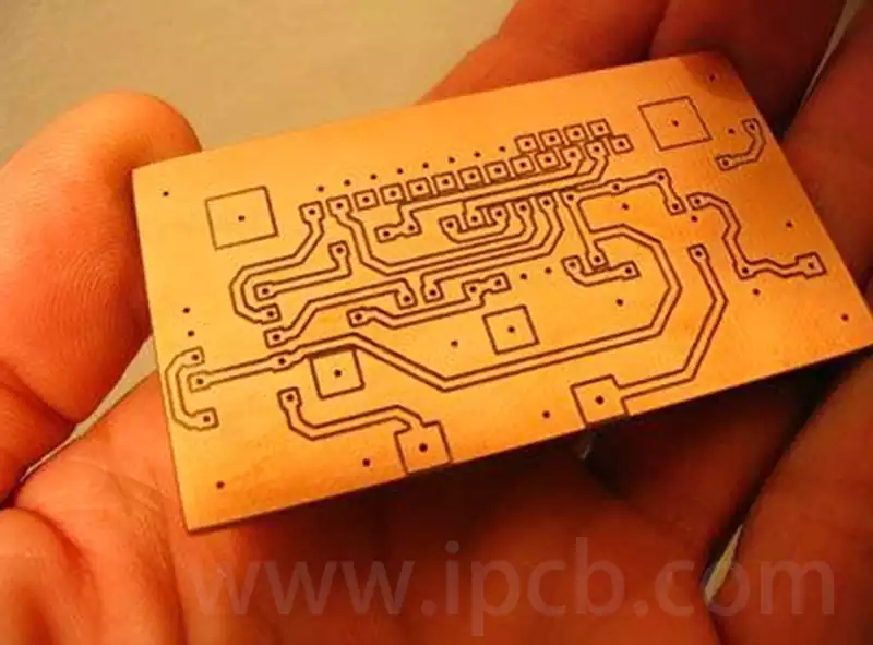
Start the laser engraving machine and etch according to the design pattern. The laser beam will accurately remove the non-circuit parts on the copper layer, exposing the substrate and forming the circuit pattern.
Chemical etching:
Place the etched circuit board into the etching solution (e.g. ferric chloride solution) to remove the copper layer that has not been engraved away by the laser. The etching process needs to control the time and temperature to avoid excessive corrosion resulting in thinning or fracture of the line.
After the etching is completed, rinse the circuit board with water to remove the residual etching solution.
Post-processing:
Check the quality of the circuit board etching, if any defects need to be repaired or reworked.
Remove the protective layer on the surface of the circuit board (e.g., transfer paper residue, photosensitive adhesive, etc.), and clean and dry it.
According to the needs of the circuit board for drilling, tinning, welding and other subsequent processing to complete the circuit board production.
Fibre laser engraving technology uses a high-power laser beam to mark, engrave or cut materials such as copper layers in PCBs. The core principle lies in the amplification of light energy through optical fibres doped with rare earth elements to generate a highly concentrated laser beam that can be precisely focused to a micron-sized spot. When the laser is applied to the copper surface, the localised high temperature causes the copper to vaporise and evaporate instantly, enabling contactless material removal. This feature gives fibre laser engraving excellent precision control, capable of completing complex circuit pattern etching, component positioning and marking and other high-precision tasks, especially suitable for high-density PCB design of micro-fine lines and dense pad processing needs.
Compared with traditional laser technologies such as CO₂ or Nd:YAG, fibre lasers significantly improve the efficiency of light-heat conversion (photoelectric conversion rate of more than 30%) through the photon-rare-earth-ion energy conversion mechanism inside the fibre, significantly reducing energy loss. Its beam quality is higher (M²<1.2), focused spot is smaller (up to 10μm level), with dynamic focusing system, it can achieve 0.01mm level line width precision etching, and at the same time to avoid edge burr or material deformation caused by thermal diffusion, which provides an efficient solution for the microvia machining, 2D code marking, anti-jamming circuit layer skeletonisation, and other processes in PCB manufacturing.
Why choose fibre laser engraving?
Among the many advantages of fibre laser engraving, its greatest strength lies in its ability to handle complex patterns. This technology enables extremely fine trajectories and detailed component layouts, as the precision of the laser minimises the risk of errors that could lead to signal loss or interference.
Another major advantage is that fibre laser engraving is a non-contact process. The laser does not physically touch the PCB, eliminating the risk of mechanical stress or damage to the board. Fibre laser engraving is therefore preferred for the manufacture of thinner or finer PCBs that could otherwise be damaged by traditional mechanical methods.
Furthermore, in terms of productivity, fibre lasers are extremely fast, making them ideal for rapid prototyping and mass production. The high power output and efficiency of the laser allows for shorter processing times than milling or even other types of lasers, without sacrificing accuracy.
Ultimately, fibre laser engraving eliminates the need for consumables such as chemical etching solutions or milling cutters. This reduces ongoing operating costs and makes the process more environmentally friendly, as there is no chemical waste to dispose of. While the upfront investment in a fibre laser system can be high, the long-term savings and sustainability benefits usually outweigh these initial costs.
Laser engraving pcb board replaces mechanical cutting with light energy and chemical etching with precise thermal etching, creating a manufacturing moat of ‘millimetre rigidity and flexibility, micron precision’ at the junction of the copper layer and the substrate. It allows flexible circuits to get rid of mechanical drilling stress risk, so that high-density wiring from the side of chemical corrosion erosion, but also no consumables, low energy consumption process characteristics, for the PCB industry to pave the way for a ‘precision and environmental protection and’ the road of transformation.