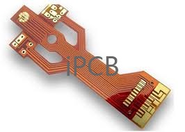
Load board pcb is a device used to test and verify the performance and functionality of electronic equipment. It can simulate real working conditions and load test the device to ensure its reliability and stability. Load boards can simulate various load conditions, evaluate power consumption, thermal management, stability, and can simulate real-world usage scenarios to test a product’s upper resistance limit and reliability. It plays a vital role in the field of manufacturing and quality control testing.
Why pcb board testing is needed? pcb is embedded in a multitude of electronic devices, and its functionality is largely dependent on the function of the pcb. It is vital to test pcb’s at the design stage and at the later stages of production as there is a lot of cost and time involved. If the pcb fails, it will have a negative impact on the business of the product in which it is embedded. Moreover, an error-free product will also improve the credibility of the brand in the market. Therefore, it is vital that pcb circuit boards are tested for functionality and part mounting.
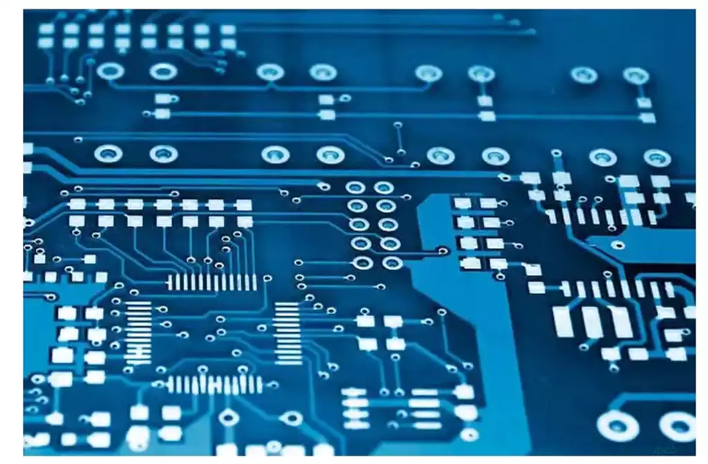
Pcb circuit board testing is necessary because if the pcb does not work properly, the electronic product may fail at any time. There are various tools and techniques to perform these tests. Signal and power integrity tests are used to solve design problems in pcb. These are pcb design analysis techniques. The test points of the board are checked with the help of certain pcb fixtures (electromechanical devices). There are automated test equipment to check the problems related to ICs and system on chip. In order to check and fix various parameters like performance, capacity, soldering issues, impedance tolerance etc., here are some of the test methods.
Functional Test:This is done in the final stage of manufacturing, if there is no problem then the product is approved otherwise the product is rejected. Therefore, at this stage, the whole product is checked as a whole rather than checking individual parameters like connectivity, board, tolerances etc. Therefore, the code for functional testing is really complex and needs to cover a lot of points which may not be arranged in the same way in each pcb. The hardware part of functional test includes functional tester, power supply, loads and probes.
In-circuit testing:This method involves testing all the components on the pcb. It identifies defective components and replaces them. The integrated circuits (ICs) are checked using certain probes. This test checks for open and short circuits and component values.
Bare Board Test: As the name suggests, a bare board is an ordinary board without any layers and mountings. The circuit connections on this artificial board are checked by applying a low voltage at specific points. This is done to identify and repair open and short circuits. Assembly level test:In this test the functionality of the assembled pcb is checked. This can be manual or automatic optical inspection (AOI).
In addition, one more type of load board pcb test is introduced, the characteristics of semiconductor load board pcb test:
Semiconductor load board pcb test methods allow complete and fixture free testing of load boards. Most professional semiconductor load board pcb testing involves testing of large load boards. Professional semiconductor load board pcb testers perform test methods that help identify defects in the process.
Semiconductor load board pcb evaluation methods can identify problems such as shorted and open pins. Specialized technicians who perform semiconductor load board pcb testing can identify weak components. Semiconductor load board pcb evaluation methods can help solve problems with components such as relays.
With a professional semiconductor load board pcb evaluation, a technician can understand IC board problems in a matter of hours. Semiconductor load board pcb testing does not involve application-specific tools.
When to use semiconductor load board pcb test equipment?
Semiconductor load board pcb’s are designed to test equipment according to a test plan. Distortion must be reduced to a low level in order to accurately analyze the performance of the device. In addition, the load board pcb must be flexible to easily handle future test requirements.
Meeting the goals of a load board test device usually requires some tradeoffs. An example of how testing is performed and the tradeoffs are shown below.
Assume that the semiconductor load board pcb test plan is to drive a clock to the IC device under test (DUT). You must first route the tester clock source to the clock pins of the DUT, which must be connected to the sockets on the semiconductor load board pcb.
To minimize distortion, you must keep the length of the clock connection to the DUT as short as possible. The clock pins should not be hardwired to the clock source as this will prevent you from using higher performance clocks for advanced testing.
The goal of semiconductor load board pcb flexibility must be achieved at the expense of a degree of accuracy. The cables and connectors required may degrade the quality of the clock signal, and this must be taken into account when using semiconductor load board pcb.
benefits of semiconductor load board pcb testing
As semiconductor designs become more complex, verifying the integrity of the IC becomes increasingly difficult. Semiconductor load board pcb testing allows manufacturers to test IC units that contain billions of circuits in a tiny area.
With semiconductor load board pcb testing, manufacturers can more accurately verify the performance of complex IC designs. Here are some of the benefits of using semiconductor load board pcb for IC device manufacturers.
Save time on continuity testing, using semiconductor load board pcb testing to verify continuity of load board performance will help save cost and time. The actual cost of verifying IC performance through standard test equipment can run into thousands of dollars per year. Companies must incur the cost of periodic performance testing to measure IC performance over the life cycle.
Using semiconductor load board pcb testing can significantly reduce the cost and time of board validation compared to validation using multi-million dollar standard test equipment.
Verification of different load board performance, a dedicated semiconductor load board pcb can be used to verify the performance of load board configurations with different measurement capabilities.
Semiconductor load board pcb is the mechanical and electrical connector between the test equipment and the IC. Using a semiconductor load board pcb, manufacturers can reliably verify the integrity and performance of an integrated circuit.
While this is common, there are several drawbacks to this practice:
High cost of testing and the use of expensive semiconductor testers (often running 24 hours a day), which affects their productivity; long development time for diagnostic tests and insufficient diagnostic capabilities: functional tests performed on semiconductor testers do not detect all possible defects on the load boards; long time to repair: when defects are detected, the testers are unable to provide accurate information about the faults; they are unable to identify defective parts and do not provide repairs Guidelines: Expert test engineers must perform in-depth, time-consuming analysis to repair the load board; Hidden faults go undetected: Defects that do not directly affect the functionality of the load board may lead to production instability or failures.
To overcome these limitations and save time and money, it is recommended that specific test methods and equipment be used to verify the performance of load boards before they are used on IC test platforms.
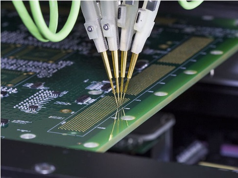
Flying probe instruments can exhaustively test all types of load boards, accurately verifying the correct functionality and parameter values of each component and network to detect each process defect or component failure. In this way, they can identify faulty components, detect process defects (e.g., open pins or short circuits), identify components that are out of specification, and “defective” components (e.g., relays) approaching the end of their useful life.
Flying probe Russian testing is performed offline, eliminating the need to spend hours on an IC tester, and load board testing can be performed without the presence of a professional engineer. Accurate diagnostic information is provided for each defect found, greatly reducing the expertise and time required to repair the load board.
Flying probe testing not only detects load board failures, but also monitors critical parameters of key components by simulating real operating conditions. For example, the “Stress Test” indicates not only the correct operation of a relay at the time of the test, but also the degradation of its contacts. Based on this information, components that may be on the verge of being damaged can be replaced preventatively, thus greatly reducing field damage and the ensuing downtime.
Semiconductor load board pcb testing does not require investment in advanced hardware and software. Experienced technicians can perform semiconductor load board pcb testing and generate results in a short period of time. Semiconductor load board pcb is performed using CAD data extracted from the load board.
All the procedures involved in semiconductor load board pcb testing can be completed in one day. Semiconductor load board pcb evaluation involves systems that help identify problems and defects. Semiconductor load board pcb testing is the starting point for more advanced testing.
Load boards are typically used to test and verify the performance and functionality of electronic devices. Its main function is to simulate real operating conditions and load test the equipment to ensure its reliability and stability under normal use.
- Simulate load: The load board can simulate various load conditions in the real working environment, such as current, voltage and other parameters. By setting different load values and states, the performance of the device under test can be evaluated under various operating conditions.
- Evaluating power consumption and thermal management: By connecting to the device under test, the load board can help evaluate the performance of the device at different power consumption levels. This is critical for thermal management design, verifying that the cooling system is adequate to keep device temperatures within safe limits in high power applications.
- Testing stability: By applying varying levels of load and continuously monitoring the response of the device under test, its stability can be verified. This helps to identify potential problems and make improvements to ensure that the product can operate reliably for a long period of time.
- Simulation of actual use scenarios: the use of load boards to create a variety of problems in the environment (such as overvoltage, overcurrent, etc.), to create a variety of extreme use of situations that may be encountered in order to test the upper limit of the product’s resistance, and also use the results of the nearly real data to make comparative judgments and then the ability to observe the upgrading to a new level.
To summarize, load board pcb is a very important and effective means of auxiliary testing, in the field of manufacturing and quality control tests can play a vital role.