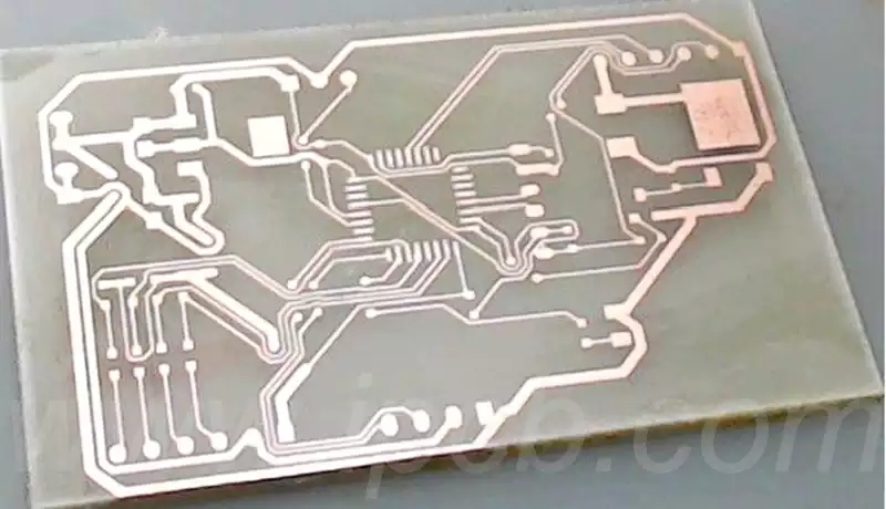
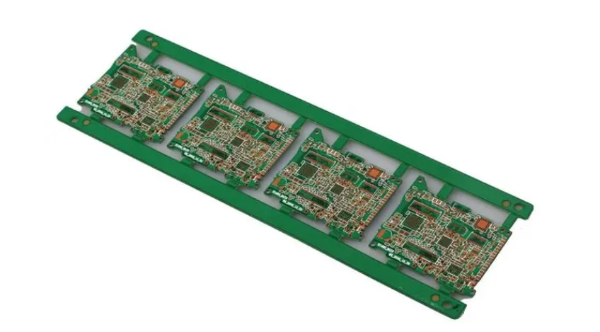
Multiwire PCB usually refer to boards that use multiple wires for signal transmission in the design of the circuit board. This technology allows more complex circuit designs to be realized in a limited space, and generally includes double-sided PCBs and multilayer PCBs. Multilayer PCBs are made of multiple layers of insulating materials and corresponding conductive layers through lamination, and usually have higher density and stronger signal processing capabilities to meet the complex needs of modern electronic devices.
The main components of a multiwire PCB include a signal layer, a power layer and a ground layer. Each layer can be independently wired and electrically connected by drilling or plating through holes. Multilayer circuit boards are often designed with additional internal power and ground layers to minimize interference problems between different signals.
Features of Multilayer Circuit Boards
- High-density wiring
Multiwire PCB is capable of high-density wiring design. By stacking multiple circuit layers, such boards can significantly reduce the length of electrical wiring and reduce losses in signal transmission, therefore improving the quality and stability of signals. This design helps to produce more compact electronic products. - Internal Power and Ground Layers
Compared to single-sided and double-sided PCBs, multiwire PCB includes internal power and ground layers in their design. These layers not only enhance power management, but also optimize interference between the power and signal directly. - Reduced wiring errors
Due to the multi-layer design, the connections between electronic components are more precise, thus reducing wiring errors due to manual soldering or connection failures. This unique design enhances product reliability and stability. - Design Flexibility
Multilayer PCB offers unparalleled design flexibility, allowing design engineers to place components in different circuit layers to meet different functional requirements.It is this flexibility that makes them ideal for designing complex electronic products. - Small size and light weight
The use of multiwire PCB can dramatically reduce the space and weight of electronic products.This is especially important for portable and high-performance devices such as smartphones and tablets. - Expanded operating temperature range
The materials and manufacturing process of multiwire PCB enables them to operate properly over a wider temperature range, which is important for certain industrial and automotive applications.
Multiwire PCB manufacturing process
- Design Phase
Before manufacturing a multiwire PCB, the designer needs to carry out a detailed schematic and layout design. This phase includes selecting components, laying out the circuit and setting parameters such as the number of layers to ensure that the functionality and performance of the circuit meets specific requirements. - Material Preparation
When manufacturing multiwire PCBs, choosing the right material is critical. Substrates are usually made of a combination of phenolic resins, glass fibers and other materials.The choice of material directly affects the insulating properties and mechanical strength of the board. - Inner Layer Fabrication
The fabrication of the inner layer of the circuit is one of the key steps in the manufacture of multilayer PCB. This process involves processes such as pattern transfer, etching and deposition to form the internal conductive circuits.Typically,a copper foil is laminated to the substrate and the pattern is formed by image transfer technology. - Lamination Process
After the inner layer has been processed, multiple inner layers need to be combined into a single unit through a lamination process. In this process, the resin between the layers is heated to a molten state by means of a hot press to form the required number and thickness of layers. At the same time, the symmetry of the layers needs to be ensured to avoid warping and deformation caused by uneven stresses. - Copper Deposition and Etching
After the inner layer is processed, the copper needs to be deposited and etched to form the desired circuit pattern. This step involves chemical copper deposition and copper plating to ensure that the thickness of the conductive layer meets the design requirements. This process is usually etched using specific chemicals. - Outer Layer Fabrication
After completing the inner layer, the outer layer of the circuit is fabricated to a higher level of manufacturing precision. The outer layer usually includes steps such as graphic transfer, etching and deposition to ensure that the board’s interfaces are capable of meeting the connection requirements of different components. - Qualification and Testing
After all the manufacturing steps are completed, the PCB needs to undergo rigorous inspection and testing to ensure its performance. This stage includes electrical performance testing, form factor inspection, etc. to ensure that each PCB can meet the technical standards and customer needs. - Post-processing
Finally, after the PCB is manufactured, it may undergo surface treatment, such as applying a protective coating to prevent oxidation and improve solderability. Common treatments include hot air leveling (HASL), electroless nickel and gold plating (ENIG) and organic coating (OSP).
How to choose the right multiwire PCB material
- Evaluate project needs
When selecting multiwire PCB materials,you first need to assess the specific needs of the project. This includes understanding the type of signals the board will carry (e.g., digital, analog, or RF signals),as well as the expected operating frequency and power requirements. For example, for high-frequency applications, materials with good signal integrity and low loss need to be selected.At the same time,it is important to consider the environmental factors of the PCB, such as temperature range and possible chemical corrosion. - Material Type
Substrate materials generally used for multiwire PCB includes FR-4, polyimide (PI), CEM-1, etc. FR-4 is the most commonly used material and is favored for its good mechanical strength and thermal stability. Polyimide, on the other hand, is suitable for higher temperatures or where bending is required. Understanding the characteristics of various materials can help designers select the right substrate while meeting electrical performance. - Design complexity
The complexity of the design of multilayer PCBs will directly affect the choice of materials required.If you need to deal with a large number of complex signals, the board needs to set up more conductive and insulating layers to maintain the signal integrity of the device and reduce electromagnetic interference. This requires materials with high standards of both mechanical strength and electrical properties.For example,the inner layers of multilayer PCBs generally require good power distribution capabilities to provide stable current and heat management. - Cost considerations
Cost is a factor that should not be ignored when choosing PCB materials. The manufacturing cost of multilayer PCBs is usually higher than that of single- or double-sided PCBs, so it is important to choose the right material within the project budget. Under the premise of meeting the performance requirements, you can consider using cost-effective materials to reduce the overall cost. In addition, companies should work with an experienced PCB supplier for advice on material selection and budget savings. - Future Scalability
When selecting materials for multilayer PCB, it is important to consider future improvements and expansions.As technology continues to advance,PCBs may be required to perform higher functionality,such as supporting more components or higher frequency signals.Therefore,selecting materials and design solutions with a certain degree of technological foresight can facilitate subsequent development.
Multiwire PCB is ideal for modern electronic product design due to their high-density wiring, internal power and ground layer design, and reduced wiring errors. Despite the complexity and high cost of its manufacturing process, product quality and performance can be effectively enhanced through reasonable material selection and optimized design.