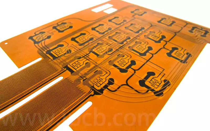
Multilayer flex pcb is formed by laminating three or more layers of single-sided or double-sided flexible circuit boards together. Through-holes are created via drilling and plating, establishing conductive pathways between different layers. This eliminates the need for complex soldering processes. Whilst the number of conductive layers in such flexible designs can be virtually unlimited, layout planning must account for the interplay between assembly dimensions, layer count, and flexibility to ensure ease of assembly.
Key Manufacturing Techniques for Multilayer Flex PCB:
Number of Layers: FPC circuit boards typically comprise 1 to 8 layers.
Substrate Materials: Common substrates include FP-4, aluminium-based materials, and PI (polyimide), with PI exhibiting a heat resistance of 260°C.
Maximum Board Dimensions: Maximum dimensions can reach 250 × 380 millimetres.
Minimum thickness: The minimum thickness achievable for FPCs is 0.057 millimetres.
Maximum Thickness: The maximum thickness is 0.7 millimetres (excluding reinforcement layers).
Copper Thickness: Copper thickness typically ranges from 1/3 ounce to 2 ounces.
Minimum Via Diameter: The minimum via diameter for laser drilling is 0.15 millimetres, and for mechanical drilling it is 0.25 millimetres.
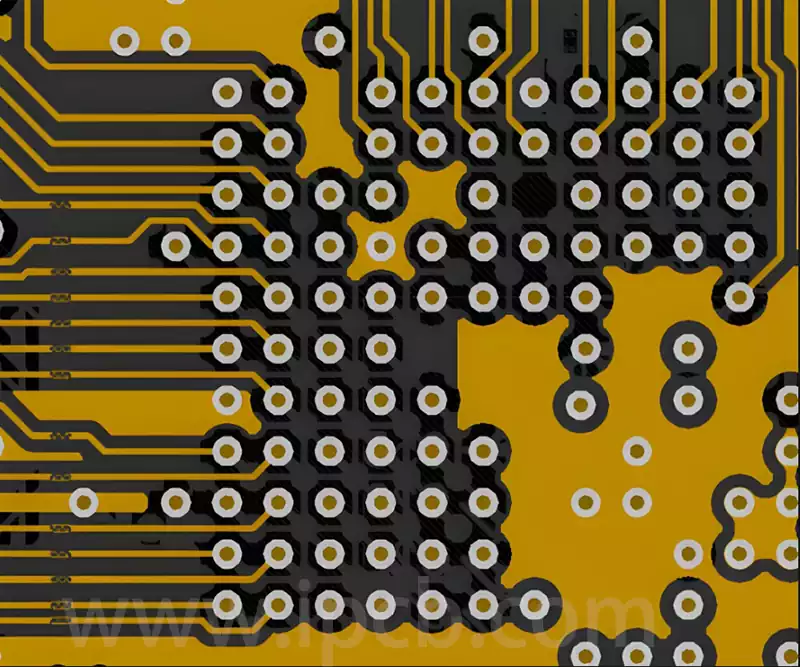
Minimum line width/spacing: Minimum line width/spacing is 2 mil/2 mil.
Maximum aspect ratio: Maximum aspect ratio is 6:1.
Surface Finishes: Common surface finishes include lead-free hot air solder level (HASL), OSP, and electroless nickel immersion gold (ENIG).
Key Processes in Multilayer Flexible PCB Manufacturing:
- Material Selection: High-quality substrate material forms the foundation of multilayer flex PCBs. Selecting appropriate polyimide or other flexible materials ensures the PCB maintains excellent electrical properties and mechanical strength during repeated bending.
- Laminating: Directly applying solder mask over the circuit pattern with tin-lead alloy layer ensures robust adhesion between the solder mask and the alloy layer. This forms either a two-layer composite structure (solder mask/SnPb alloy layer/copper circuit pattern) or a three-layer composite structure (solder mask/SnPb alloy layer/copper circuit pattern/solder mask).
- Drilling: Utilising laser drilling technology to precisely create micro-apertures within the PCB. This high-precision drilling method provides interlayer connection pathways without damaging surrounding materials.
- Plating: Depositing a uniform copper layer on the bore walls via chemical plating or electroplating to achieve excellent electrical conductivity. This step is crucial for ensuring connection stability and reliability.
- Photolithography: Transferring circuit patterns onto the PCB using photolithography, a high-precision pattern transfer technique guaranteeing accuracy and consistency.
- Etching: Excess copper is removed via chemical etching, leaving the desired circuit pattern. This step requires precise control of etching duration and solution concentration to prevent over-etching or under-etching.
- Testing and Verification: Rigorous electrical testing and mechanical bending tests are conducted on the finished PCB to ensure reliability in practical applications. Additionally, simulation analysis can help predict potential issues and enable pre-emptive optimisation.
Limitations of Multilayer Flex PCB:
High Initial Costs: The design and manufacturing costs of FPCs are initially substantial, particularly for customised requirements. This renders them less cost-effective than rigid PCBs for small-batch production.
Modification Difficulties: Once manufactured, adjustments or repairs to FPCs are complex, necessitating redesign of the master artwork or photoplotting programme. The removal and restoration of protective films further complicates repairs.
Dimensional constraints: FPCs produced via intermittent processes face limitations imposed by existing manufacturing equipment, preventing unlimited extension or widening.
Fragility: FPCs demand high operator skill levels; improper handling readily causes damage, particularly during soldering and rework. Professional execution is essential to prevent circuit destruction.
Despite these manufacturing challenges and limitations, multilayer flex pcb is increasingly prevalent in modern electronic devices due to their unique advantages: flexibility, miniaturisation, and high integration. Ongoing technological advancements will further optimise future manufacturing processes, reducing costs, enhancing modifiability, and overcoming dimensional constraints to broaden the application scope of multilayer flexible pcb boards.