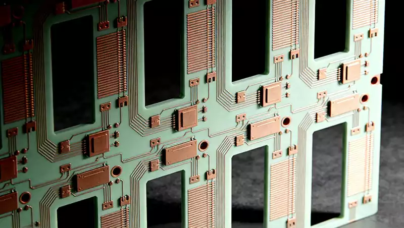
Ceramic circuit boards, owing to their high thermal conductivity and excellent insulation properties, have become a key material in high-end electronics. However, their high cost has hindered widespread adoption.
Reasons for the High Cost of Ceramic Circuit Boards
The high cost of ceramic circuit boards is not caused by a single link but results from the superposition of multiple factors such as raw materials, processes, equipment, and yield. Precisely identifying the root causes of costs is essential for achieving targeted cost reduction.
Raw material costs account for over 40% and are the core contributing factor for high costs. Core raw materials for ceramic circuit boards, such as aluminum nitride and high-quality glass powders, have long relied on imports, keeping prices high. The use of precious metal pastes (e.g., gold paste) further drives up costs. For example, in traditional LTCC (Low-Temperature Co-fired Ceramic) processes, the cost of gold paste accounts for over 60% of the total material cost of the substrate. The complexity of processes adds to cost pressures. Whether it is the high-temperature energy consumption of high-temperature co-firing (HTCC) or the multiple photolithography and electroplating steps in direct plating copper (DPC), there are issues of long processes, high energy consumption, and significant material waste. The scrap rate due to layer alignment deviations in traditional multilayer ceramic circuit boards can reach 30%. Production equipment relies on imports, with key equipment such as tape casters and high-precision sintering furnaces costing millions of yuan to purchase, and subsequent maintenance and calibration costs continuously consuming funds. In addition, inefficient manual inspection, inconsistent standards leading to yield fluctuations, and the inability to achieve economies of scale in small-batch production further amplify unit costs.
Strategies for Reducing the Cost of Ceramic Circuit Boards
1.Raw Material Optimization
The core of raw material cost reduction lies in “substitution” and “material selection.” Under the premise of ensuring performance, low-cost domestic materials are used to replace imported materials, and cost-effective raw material combinations are used to replace precious metals.
Substitution with domestic materials has made substantial breakthroughs and has become the core approach to raw material cost reduction. In the past, LTCC green tapes and matching glass powder pastes were long monopolized by companies such as Ferro and DuPont in the United States. The unit price of imported green tapes could reach 800 – 1200 yuan per square meter, and the price of matching gold paste was as high as tens of thousands of yuan per kilogram. Nowadays, domestic institutions and enterprises such as China National Building Material Group Academy and Guangdong Fenghua Advanced Technology have developed TD17 and TD20 series domestic LTCC green tapes. Their performance indicators (such as dielectric constant and sintering shrinkage rate) have reached or exceeded those of imported products, and their unit price is only 1/2 – 2/3 of that of imported products. In terms of conductive paste substitution, domestic silver paste has maturely implemented the technology of preparing a surface gold layer through chemical plating, which can completely replace the expensive gold paste used in traditional LTCC processes, directly reducing the total material cost of the substrate by 50% – 70%, with conductive performance and corrosion resistance no less than those of gold paste.
In the selection of substrate materials, precisely matching application scenario requirements can further compress costs. For ordinary medium-power scenarios (such as household LED drive modules), low-cost alumina (Al₂O₃) ceramics can meet the requirements, and their raw material cost is only 1/3 – 1/2 of that of high-thermal-conductivity aluminum nitride (AlN) ceramics. For high-thermal-conductivity requirement scenarios (such as power modules in new energy vehicles), there is no need to use aluminum nitride for the entire board. A composite structure of “alumina + local aluminum nitride” can be adopted—embedding aluminum nitride substrate in the core heat dissipation area and using alumina in other areas. This can not only ensure the heat dissipation performance of key parts but also reduce the overall material cost by more than 30%. In addition, optimizing the raw material ratio can also improve utilization. For example, adding 5 wt% of low-shrinkage additives to ceramic pastes can reduce warping and cracking during sintering, increasing raw material utilization from the traditional 85% to over 95%, indirectly reducing unit costs.
2.Process Innovation
Processes are the core link in cost control. By simplifying processes and integrating new technologies, energy consumption can be significantly reduced, the number of steps can be decreased, and the finished product rate can be improved.
There are significant cost differences among different process routes. Precisely matching production capacity and performance requirements to select processes is the primary principle for process cost reduction. For mass production scenarios (such as automotive electronic ceramic circuit board with an annual production capacity of over 1 million pieces), the mature DBC (Direct Bonded Copper) process is preferred. This process only requires three steps: “ceramic circuit board pretreatment – copper cladding – high-temperature welding,” with low energy consumption and little material waste. The unit cost is much lower than that of the AMB (Active Metal Brazing) process, and it can meet the temperature and thermal conductivity performance requirements of most power modules. For high-precision, small-batch customization scenarios (such as ceramic circuit boards for aerospace applications), the DPC process can be selected. By optimizing parameters such as the thickness of the photoresist coating and the electroplating current density, the copper layer material waste can be reduced from the traditional 25% to below 10%, balancing precision and cost.
The integration of emerging technologies provides new paths for process cost reduction. The combination of light-curing 3D printing and co-firing technology is a typical example. Traditional multilayer ceramic circuit board production requires the production of multiple sets of molds for punching and positioning of green tapes. The mold cost accounts for more than 40% of the R&D cost, and layer alignment deviations can easily lead to an increase in the scrap rate. Light-curing 3D printing can directly form multilayer interconnection channels and embedded heat dissipation holes without the need for molds, shortening the R&D cycle from 2 – 3 months to 7 – 10 days and reducing R&D costs by 60%. At the same time, the layer alignment deviation is reduced from 22 μm to 8 μm, and the interconnection success rate is increased from 60% to 92%, significantly reducing waste losses. In addition, optimizing sintering process parameters can also significantly reduce costs. For example, reducing the sintering temperature of HTCC from 1600°C to 1450°C can reduce energy consumption by more than 30%. At the same time, it can match the sintering temperature of silver conductors, avoiding the oxidation waste of precious metals and further compressing material costs.
3.Equipment Upgrades
The automation upgrade and domestic substitution of production equipment are key to reducing labor costs and improving production stability.
Replacing manual labor with automated equipment is a key measure to reduce labor costs and improve production stability. Traditional ceramic circuit boards inspection relies on nearly a hundred people working in three shifts for manual inspection. Not only is the per capita inspection efficiency only 500 pieces per day, but there are also issues of inconsistent standards and a high miss rate (which can reach 5% – 8%). After adopting automatic optical inspection equipment based on the “Qingque” and “Yuxia” dual large models, the inspection accuracy exceeds 95%, the miss rate is below 0.5%, and the daily inspection volume of a single device can reach over 5,000 pieces, with an efficiency increase of 10 times. At the same time, it helps increase the yield of medium- and high-end products by 20% and shorten the verification cycle of complex products by 35%, indirectly reducing rework and scrap costs caused by missed inspections.
The application of domestic equipment can significantly reduce procurement and maintenance costs and break the price monopoly of imported equipment. In the past, the procurement cost of key imported equipment such as high-precision tape casters and sintering furnaces was as high as millions of yuan, and the subsequent maintenance and calibration costs were 100,000 – 200,000 yuan per year. Nowadays, domestic equipment has achieved technological breakthroughs. The unit price of domestic high-precision tape casters is only 1/2 – 2/3 of that of imported equipment, and the energy consumption of domestic sintering furnaces is 15% – 20% lower than that of imported equipment, with maintenance parts supplied in a timely manner and costs reduced by more than 50%. In addition, upgrading existing equipment can also achieve cost reduction. For example, introducing zone control temperature technology in traditional sintering furnaces to improve the temperature uniformity inside the furnace can reduce the scrap rate due to uneven sintering from 12% to below 5%, further compressing costs.
4.Yield Improvement
The yield directly determines the unit cost. Through AI-enabled inspection and full-process quality control, the scrap rate can be minimized.
AI visual inspection technology has become the core means of improving yield, effectively solving the problems of low efficiency and inaccurate defect identification in traditional inspection methods. The “Qingque” large model developed by Northeastern University can accurately identify more than 10 common defects in ceramic packaging substrates such as magnetic leakage, short circuits, foreign objects, and interlayer peeling, with an identification accuracy exceeding 98%. The “Yuxia” large model can generate a large number of defect samples based on normal samples, solving the problem of scarce defect samples and difficult model training for ceramic circuit boards. The dual models work together to form a complete closed loop of “data generation – defect detection – process optimization.” In the practical application of a ceramic circuit board enterprise, they have inspected 110,000 products, reducing the scrap rate from 15% to below 8%, effectively reducing rework and scrap costs caused by defects.
Establishing a full-process quality control system is the foundation for ensuring stable yield. Clear quality standards and inspection procedures should be set for each link from raw material warehousing inspection, in-process inspection of each step to finished product outgoing inspection to prevent unqualified products from entering the next process and reduce invalid cost inputs. For example, during raw material warehousing, the purity and particle size distribution of ceramic powders are detected using a laser particle size analyzer to ensure a purity of ≥99.9% and a particle size deviation of ≤5 μm, which can avoid sintering defects caused by raw material impurities. During the green tape forming process, detecting the thickness uniformity (deviation ≤2 μm) and flatness of the green tape can reduce warping problems during subsequent lamination and sintering. Before the finished products leave the factory, multiple performance tests such as high-voltage insulation tests and thermal conductivity tests are conducted to ensure that the products meet application requirements and avoid after-sales costs caused by finished product quality problems.
5.Supply Chain Optimization
Fine management of the supply chain can reduce procurement costs through economies of scale and resource integration.
Expanding production scale is the basis for achieving economies of scale and is also the core logic of supply chain cost reduction. When the production capacity of ceramic circuit boards increases from 100,000 pieces per year to 1 million pieces per year, fixed and variable costs such as equipment depreciation, personnel costs, and raw material procurement can be amortized over more products, and the unit cost can be reduced by 30% – 40%. For example, when an enterprise produces 100,000 ceramic circuit boards per year, the unit equipment depreciation cost is 20 yuan per piece; when the production capacity increases to 1 million pieces per year, the unit equipment depreciation cost drops to 2 yuan per piece, a decrease of 90%.
Establishing long-term and stable cooperative relationships with raw material suppliers can help obtain more favorable procurement prices through centralized procurement and signing long-term supply contracts. For example, a ceramic circuit board enterprise signed a three-year long-term supply contract with a domestic ceramic powder supplier and concentrated the procurement volume to over 50 tons, reducing the procurement price by 15% compared with sporadic procurement. At the same time, it ensured a stable supply of raw materials and avoided production shutdowns due to raw material shortages—a production shutdown for one day could result in losses of tens of thousands of yuan for the enterprise in terms of equipment idleness and personnel on standby. In addition, optimizing the supply chain layout can also reduce costs. Choosing nearby raw material suppliers and processing manufacturers can reduce logistics transportation costs and transportation losses. For example, transferring raw material suppliers from abroad to domestic surrounding areas can reduce logistics costs by more than 40% and transportation losses from 3% to below 0.5%.
6.Design Optimization
Optimization at the product design stage can reduce cost waste from the source and avoid unnecessary investments in subsequent processes.
Optimization at the product design stage can reduce cost waste from the source and avoid unnecessary investments in subsequent processes. The cost reduction potential of this link is often overlooked. During the early design stage, R&D personnel need to fully communicate with downstream application enterprises to clarify the actual application requirements of the products and avoid over-design. For example, in non-extreme high-temperature (≤150°C) scenarios, there is no need to select high-end ceramic circuit boards with a Tg value of ≥250°C. In ordinary power (≤50W) scenarios, the line precision requirement can be relaxed from ±5 μm to ±10 μm, reducing the difficulty and cost of the photolithography process, and the unit processing cost can be reduced by more than 20%.
Optimizing the circuit layout and structural design can also achieve cost reduction. Reasonably planning the line width and spacing can appropriately increase the line spacing while meeting the current carrying requirements, reducing the amount of ceramic material used. Optimizing the via layout and adopting a “fewer but larger” via design instead of a “more but smaller” one can reduce the difficulty of drilling and via filling processes, improve processing efficiency, and reduce material waste. Adopting modular design and integrating circuits with different functions (such as drive circuits and heat dissipation circuits) onto one substrate can reduce the number of substrates and improve integration, reducing overall assembly costs. For example, a power module for new energy vehicles integrated three independent ceramic circuit boards into one integrated substrate through modular design, not only reducing the procurement cost of substrates but also reducing assembly steps, resulting in an overall cost reduction of 25%.
The cost reduction path for ceramic circuit boards is not a “subtraction” that sacrifices performance but a “multiplication” that achieves value reconstruction through collaborative innovation across the entire chain. With the maturity of domestic material technology, the popularization of emerging processes, and the advancement of large-scale production, the cost of ceramic circuit boards will continue to decrease, and their application scenarios will also expand from high-end fields to medium- and low-end markets, driving the electronic industry towards higher performance and more green and energy-saving development.