Multilayer pcb board lamination is an electronic manufacturing technology designed to combine multiple layers of conductive and insulating materials through specific process steps to form multilayer circuit boards.
Advantages
Multilayer PCB lamination process can provide higher circuit density. Compared to traditional single-layer circuit boards, the pcbs can accommodate more electronic components and connections, allowing for more complex functional integration. This is critical for modern electronics, which often require more functionality and performance in a limited space.
The pcb lamination process also improves circuit stability and reliability. Due to the stacked design of multilayer PCB, electronic components are more tightly connected to each other, reducing interference and loss in signal transmission. In addition, it also has better anti-interference performance, and can effectively resist external electromagnetic interference and noise. These features make the boards outstanding in high frequency, high-speed transmission, and other application areas.
In addition, it can also improve the thermal performance of the product. With the increase in power consumption of electronic products, the heat dissipation problem has become an important factor in restricting product performance. It stacking design can effectively improve the heat dissipation effect, through the reasonable thermal conductivity design and heat dissipation channel, the heat will be rapidly conducted to the external environment, to maintain the normal operating temperature of the electronic components, to improve the stability and life of the product.
The PCB board lamination process can also simplify the product manufacturing process. Compared to the use of multiple single-layer circuit boards for assembly, multilayer pcb can be electronic components directly welded to different levels of circuit boards, reducing the use of connecting wires, simplifying the assembly process, and improving production efficiency. This is especially important for mass production and rapid delivery requirements.
pcb lamination process Flow:
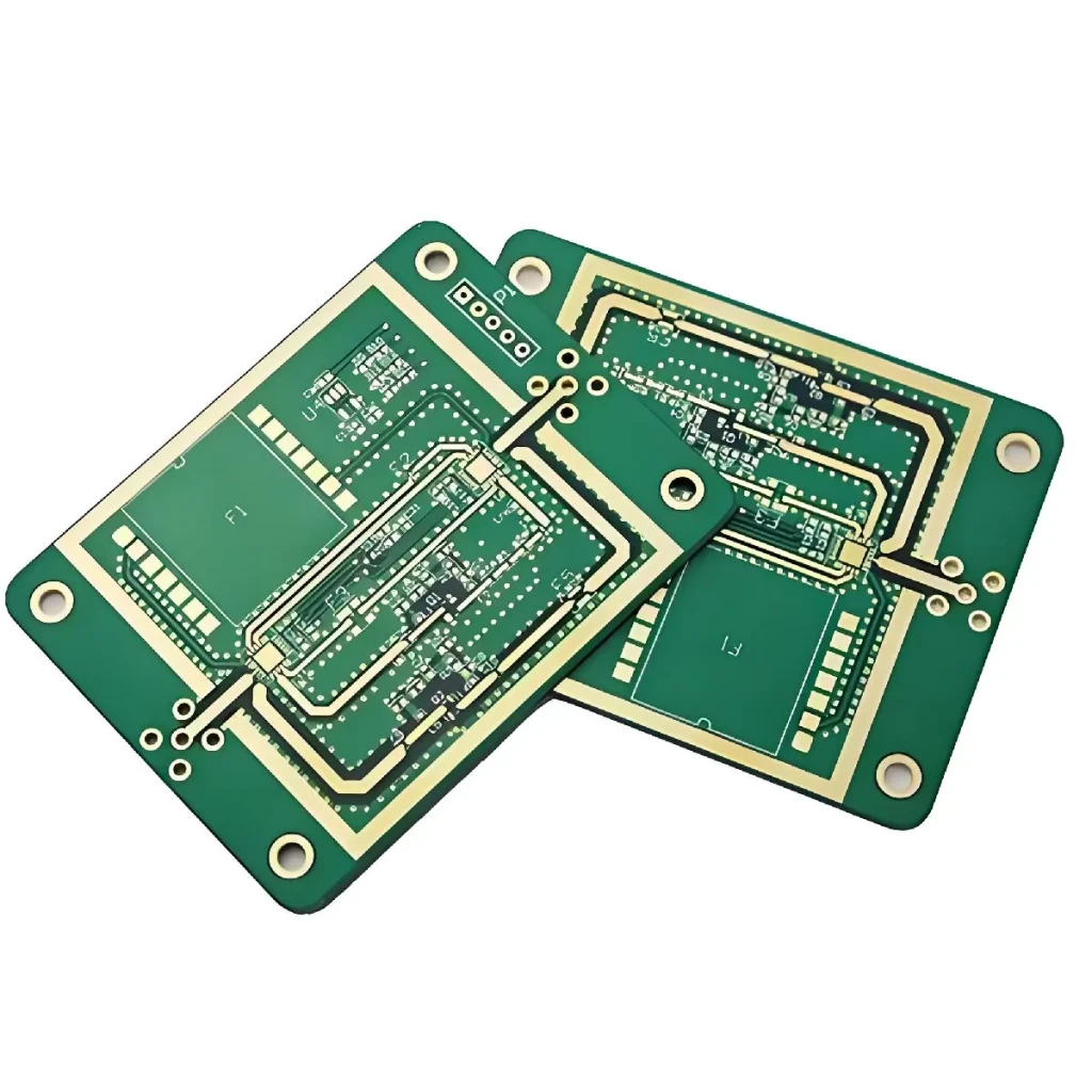
Inner layer fabrication: first, the inner circuit pattern is created according to the design requirements. This typically involves covering the copper foil with a dry film and then transferring the circuit pattern to the copper foil through steps such as exposure and development. Next, the inner layer is etched to remove excess copper foil and form the desired circuit pattern.
Pre-lamination: Before lamination, the inner laminate needs to be treated to ensure a good bond between the layers. This may include cleaning, roughening, etc. of the inner laminate to increase the bonding between the layers.
Lamination process: Multiple inner laminates are stacked alternately with insulating materials (e.g. prepregs) and placed in a hot press for lamination. During the lamination process, the insulating material is heated and pressurized so that it melts and fills the gaps between the layers to form a tight bond. At the same time, the resin cures during the hot pressing process, which further enhances the bonding between the layers.
Post-processing: After the lamination is completed, the multilayer board needs to undergo post-processing, such as drilling, deburring, and plating. These steps are intended to complete the final processing of the multilayer board to meet the design requirements.
It is important to note that the control of parameters such as temperature, pressure, and time is critical in the multilayer PCB lamination process. These parameters will directly affect the quality of the lamination and the performance of the multilayer board. Therefore, in the actual production process, these parameters need to be strictly controlled and adjusted according to the specific circumstances.
In electronic manufacturing, the status of the multilayer PCB lamination process is pivotal. It is one of the key technologies for realizing high performance, high integration, thin and light, and miniaturization of electronic devices. From smartphones, tablet PCs to automotive electronics, and medical devices, to aerospace and military fields, multi-layer PCB lamination process plays an irreplaceable role.