What is multilayer pcb?A multilayer circuit board is a pcb board consisting of two or more electrically conductive layers stacked by insulating layers. It is a widely used basic component in electronic devices and consists of multiple layers, each of which contains circuit lines and connecting components. It is widely used in high-end electronics because it offers higher circuit density and better electromagnetic compatibility than single-layer circuit boards.
How to make multilayer pcb?
The PCB multilayer production process consists of four stages: design, material preparation, manufacturing process and post-processing. Each of these stages is interconnected and interacts with each other, and the absence of any one of them will directly affect the performance and quality of the final product.
Design phase
- Preliminary design: The first step of PCB design is to determine the circuit diagram, component selection and circuit connection according to the functional requirements of the product.
- PCB layout. Layout design is the first step after the completion of the circuit design, you need to determine the approximate size and shape of the PCB board, as well as the general location of various components on the board.
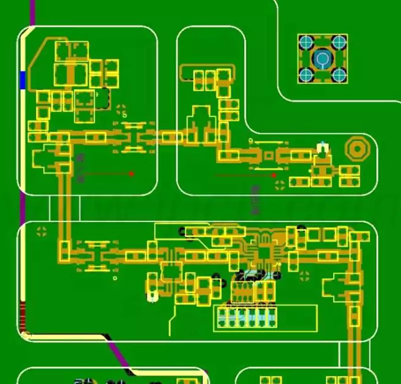
- Alignment design. The designer needs to design the circuit connections and paths in each layer of the PCB, this process is called alignment design.
Material preparation stage
- Selection of base material. Before starting the production of multilayer boards, you need to select the appropriate substrate, usually used is a glass fiber board.
- Make copper foil. Copper foil is the most important conductive material in the PCB substrate, according to the PCB design requirements for thickness selection and production.
- Make photolithography film. Photolithography film is a key tool in the production of circuit board, which transforms the circuit design drawing into a physical object for subsequent photolithography steps.
Manufacturing process
- Photolithography. Photolithography is the most important step in the process, which transfers the designed circuit graphics to the copper foil of the PCB.
- Etching. The etching process removes the unwanted copper foil to form the circuit board.
- Drilling. Holes are drilled to allow the circuitry to be connected between the layers.
Post-processing stage
1.Surface treatment. Surface treatment includes gold plating, silver plating, tin spraying, etc., which can enhance the conductivity and corrosion resistance of the PCB surface.
2.Testing. Testing is to ensure the quality and performance of the PCB, including electrical testing and reliability testing.
3.Packaging. The finished PCB is packaged to protect it from damage during transportation and use.
Multilayer circuit boards are generally defined as high multilayer circuit boards of 10 to 20 layers or more, which are more difficult to process than traditional multilayer circuit boards, and their quality and reliability requirements are high, and they are mainly used in communication equipment, high-end servers, medical electronics, aviation, industrial control, military and other fields. In recent years, the application of communications, base stations, aviation, military and other areas of high-level board market demand remains strong, and with the rapid development of China’s telecommunications equipment market, high-level board market prospects are favorable.
The main difficulties in the production of high multilayer circuit board:
Difficulty of interlayer alignment
Due to the number of layers of high-level boards, the customer design side of the PCB layers of the alignment requirements are increasingly stringent, usually inter-layer alignment tolerance control ± 75μm, taking into account the design of high-level board unit size is larger, the graphics transfer workshop environment temperature and humidity, as well as the inconsistency of the different core board layer expansion and contraction of the misalignment brought about by the superposition of the interlayer positioning methods and other factors that make the high-level board of the interlayer alignment control is more difficult.Difficulty of inner layer line productionHigh-level boards use high TG, high-speed, high-frequency, thick copper, thin dielectric layer and other special materials, the inner layer line production and graphic size control puts forward high requirements, such as the integrity of impedance signal transmission, increasing the difficulty of the inner layer line production.Line width line spacing is small, open short circuit increased, micro-short increased, low pass rate; fine line signal layer is more, the inner layer of AOI leakage rate increased; inner core plate thickness is thin, easy to crease lead to poor exposure, etching over the machine is easy to roll the plate; high-level board most of the system board, unit size is larger, in the finished product scrap cost is relatively high.Pressing production difficulties
Multiple inner core boards and semi-cured sheet stacking, press production is prone to produce slippery boards, delamination, resin voids and bubble residue and other defects. When designing the laminated structure, it is necessary to fully consider the heat resistance of the material, voltage resistance, the amount of glue filling, and the thickness of the medium, and to set a reasonable program for press lamination of high-level boards. With more layers, the control of rise and shrinkage and the amount of size factor compensation can not maintain consistency; the thin insulation layer between the layers will easily lead to the problem of interlayer reliability test failure.
Difficulties in drilling productionThe use of high TG, high-speed, high-frequency, thick copper special plates increases the difficulty of drilling roughness, drilling burrs and de-drilling dirt.More layers, cumulative total copper thickness and board thickness, drilling easy to break the knife; more dense BGA, narrow hole wall spacing caused by CAF failure; due to the board thickness is easy to lead to slant drilling problems.Advantages.
Because multilayer circuit boards can be arranged on the same board with multiple circuit layers, the size of the board can be greatly reduced, making electronic products thinner and more portable. At the same time, it can also reduce the length of signal lines, reduce the signal transmission delay, improve the working speed and stability of the circuit.
Good anti-interference performance. The insulation between different layers can effectively isolate the signal lines and power lines, reducing the interference between each other.This is especially important for high-frequency circuits and analog circuits to provide more stable and reliable signal transmission.
Helps to improve the heat dissipation performance of the circuit.Because of the large heat dissipation area, heat dissipation can be improved by adding heat dissipation layers or holes. This is especially important for electronic devices with high power consumption, which can effectively reduce the temperature and extend the service life of electronic products.
However, it also has some disadvantages. The first is the higher manufacturing cost.Compared with single-layer circuit boards, this type of circuit board requires more processes and materials, so the manufacturing cost will be relatively high. Secondly, the design complexity is higher.Since multilayer circuit boards involve wiring and connections between multiple circuit layers, the design process is relatively complex and requires more specialized skills and experience.
Multilayer pcb, as an indispensable key component in modern electronic devices, are gradually becoming the mainstream choice in high-end electronic products with their efficient and compact circuit solutions.Despite higher manufacturing costs and greater design complexity, the size reduction, performance improvement and reliability enhancement they bring have led to the widespread use of multilayer circuit board in communication equipment, high-end servers, medical electronics, aerospace, industrial control, military and other fields.