PCB antenna, also known as printed circuit board antenna, is a form of antenna in which the antenna is printed directly on a PCB (printed circuit board). This type of antenna plays an increasingly important role in modern wireless communication devices, especially in mobile devices, IoT devices and wireless sensor networks, where it is widely used due to its compactness, lightweight and low cost.
Design elements of PCB antenna
- Frequency: The frequency of a the antenna determines the range of signals it can send and receive. The frequency is related to the physical size of the antenna, and lower frequencies require longer antenna lengths.
- Gain: The gain determines the size of its radiated power. The higher the gain, the farther the antenna radiates.
- Directionality: The directionality determines the direction range of its radiated and received signals. The stronger the directionality, the better the signal transmission effect of the antenna in a particular direction.
- Impedance matching: Impedance matching is required between circuit board antenna and radio frequency transmitter or receiver to ensure maximum efficiency of signal transmission.
Antenna part of the circuit design
- Matching circuit design
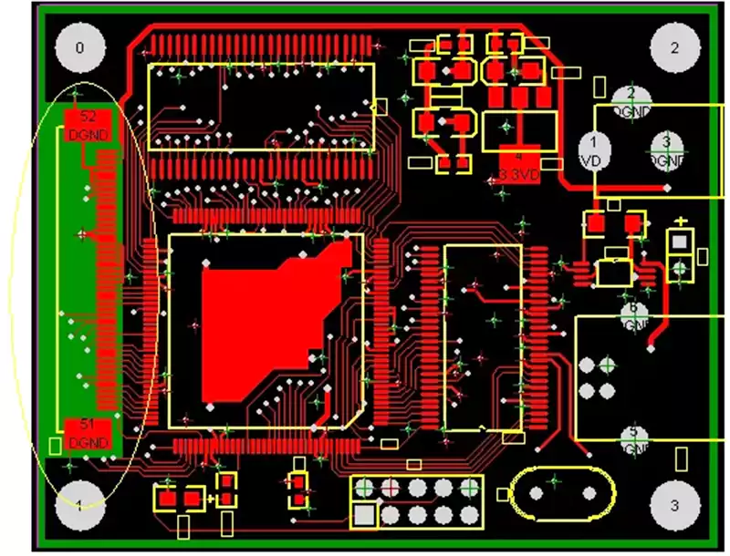
In the schematic design, it is necessary to reserve a π-type network between the antenna and the RF output pin of the module. The impedance of the antenna is affected by the PCB laying, the installation of the antenna and the surrounding metal, etc. This network is reserved to match the antenna to 50 ohms when it deviates seriously from the 50 ohms impedance. x1, x2, x3 are reactance components, if the antenna is a standard 50 ohms impedance, then x2, x3 can be left un-welded, and x1 is connected to a 220PF capacitor or a 0 ohms resistor. During circuit board design, these three devices have been placed as close as possible to the RF output pin of the module and connected with short and straight transmission lines. Do not pave the ground in the 1.5mm area around the matching components to reduce the impact of parasitic parameters on the matching circuit.
2.Microstrip line design
In PCB design, as most of the antenna and module output impedance is 50 ohms, in order to minimize the reflection of energy in the transmission process, RF output pins to the antenna between the PCB leads should be 50 ohms microstrip line. The commonly used board is FR4 (dielectric constant 4.2-4.6). According to experience, when the line width is about 2.2 times the distance of the microstrip line from the reference layer, the characteristic impedance of the microstrip line is about 50 ohms. For specific design, it is recommended to use microstrip line impedance control tools (ADS, txline, etc.) to calculate and complete the design of the microstrip line through actual debugging. As shown in the figure below, the grounding layer under the microstrip line must be a complete ground, and more grounding perforations are needed on both sides of the microstrip line.
- The effect of metal on the antenna
Circuit board factory speak if the antenna near the metal material objects, metal can reflect electromagnetic waves, not only will affect the actual use of the antenna space, increase the loss resistance of the antenna, reduce the radiation efficiency, and lead to the deterioration of the antenna radiation performance. When installing the antenna, pay attention to:
a: The antenna should be at least 5mm from the battery;
b: The antenna should be at least 4mm from the shielding shell;
c: On occasions where the shell needs to be installed, do not use spray paint or plating with metallic components on the surface of the shell.
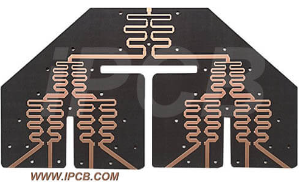
Common circuit board antenna types
- Linear polarized antennas:including unipolarized and dual-polarized antennas, suitable for most wireless communication applications.Common linear polarized antennas include half-wavelength dipole antennas and patch antennas.
- Circularly polarized antennas: can achieve omnidirectional radiation and receive signals. Common circularly polarized antennas are spiral antenna and yagi disk antenna.
- Radio Frequency Identification (RFID) antenna: Used for wireless identification and Internet of Things applications. Common RFID antennas include large loop antennas and folded antennas.
- Broadband antenna: suitable for applications that need to cover multiple frequency bands, common broadband antennas are Vivaldi antenna and fin antenna.
Ceramic antenna and pcb antenna advantages and disadvantages comparison
Ceramic antenna:It is a kind of miniaturized antenna suitable for Bluetooth devices, which is divided into block ceramic antenna and multilayer ceramic antenna.
Ceramic antenna occupies very little space and has better performance;
Narrow bandwidth, more difficult to do multi-band;
Effectively improve the integration of the motherboard, and can reduce the antenna on the ID limit;
Need to import the design at the beginning of the definition of the motherboard.
Ceramic Antenna
Block antenna:
Use high temperature to sinter the whole ceramic body at one time and then print the metal part of the antenna on the surface of the ceramic block.
Multi-layer antenna:
Low temperature co-firing method is used to sinter multiple layers of ceramics in place and then sintered at high temperature, so the metal conductor of the antenna can be printed on each layer of ceramic media according to the design needs.
In this way, the antenna size can be effectively reduced, and can achieve the purpose of hiding the antenna.
Because the ceramic itself dielectric constant is higher than the pcb circuit board, so the use of ceramic antenna can effectively reduce the size of the antenna under the condition of guaranteeing the performance of the antenna.
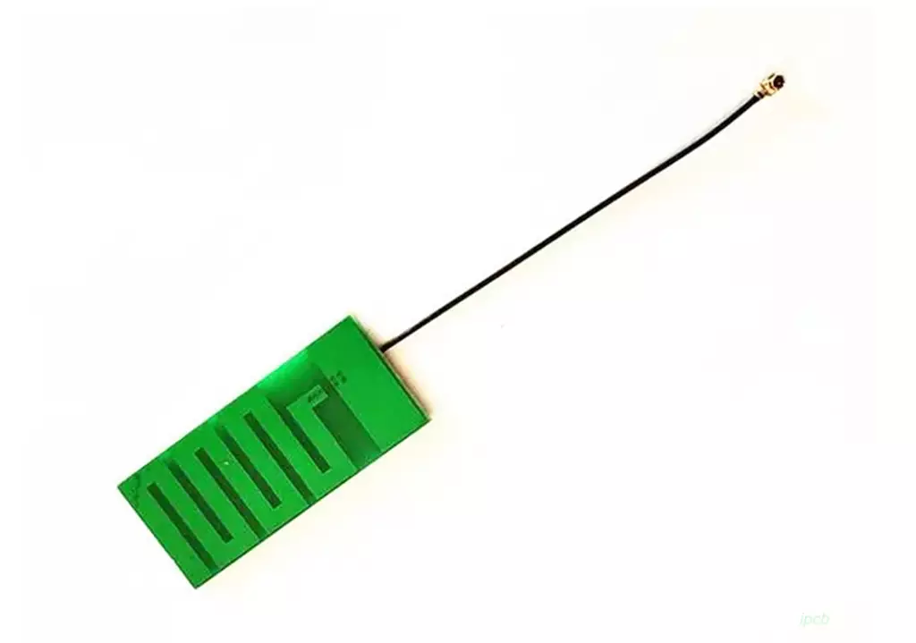
PCB Antenna
It is the part of PCB used for wireless reception and transmission.
When transmitting, it converts the high-frequency current from the transmitter into space electromagnetic waves;
When receiving, it converts the electromagnetic wave intercepted from space into high-frequency current and sends it to the receiver.
Advantages and disadvantages analysis
Advantages: less space occupation, low cost, do not need to assemble the antenna separately, not easy to touch the damage, easy to assemble the whole machine;
Disadvantages: a single antenna field pattern is difficult to do round, high insertion loss, relatively low efficiency, easy to be interfered with on the motherboard.
With the rapid development of wireless communication technology, PCB antenna has become an indispensable part of modern wireless communication equipment with its compact, lightweight and low-cost features. Whether it is mobile devices, IoT devices or wireless sensor networks, it plays an important role and brings us a more convenient communication experience.