Description
The processes involved in manufacturing printed circuit boards (PCBs) are time-consuming and complex. Excellence in these processes is a must since PCBs are the backbone of all electronic circuits. PCBs come in several different forms. Rigid (hard board), flexible (copper and coverlay), rigid-flex (integrated rigid and flexible circuits) are the most common. This publication will focus on the processes used to produce rigid PCBs, which are categorized into 3 types: single-sided, double-sided, and multi-layer. The most commonly used material for rigid PCBs is based on a fiberglass called FR-4. Other options are used such as paper phenolic paper for low-cost commercial products. Teflon or polytetrafluoroethylene are used for high-performance, high-frequency designs. Flexible, rigid-flex typically use polyimide-based substrates.
PCB Board Fabrication Process
Now, let’s get started with the pcb board fabrication process. The manufacturing process of printed circuit boards can be summarized in the following 13 steps.
1- Design
Before the manufacturing process begins, the PCB needs to be designed/laid out by a CAD operator based on a working circuit schematic. Once the design process is complete, a set of documents is provided to the PCB manufacturer. Included in the documentation are Gerber files which include layer-by-layer configuration, drill files, pick and place data, and text annotations. Processing prints provide processing instructions critical to manufacturing, all PCB specifications, dimensions, and tolerances.
2-Pre-manufacturing preparation
Once the PCB house receives the file package from the designer, they can begin creating a pcb board fabrication process plan and artwork package. The manufacturing specification will determine the plan by listing things like material type, surface finish, plating, work panel array, process routing, etc. In addition, a set of physical artwork can be created through a film plotter. The artwork will include all layers of the PCB as well as artwork for solder mask and terminology markings.
3-Material preparation
The PCB specifications required by the designer determine the type of material, core thickness, and copper weight used to begin the material preparation work. Single-sided and double-sided rigid PCBs do not require any inner layer processing and go directly to the drilling process.
If the PCB is multi-layer, similar material preparation will be carried out, but in the form of inner layers, which are usually much thinner and can be built up to the predetermined final thickness (stack-up). A common production panel size is 18″x24″, but any size can be used as long as it is within the PCB manufacturing capabilities.
4-Multilayer PCB Only – Inner Layer Processing
After the inner layers are prepared with the proper size, material type, core thickness, and copper weight, they are sent to be drilled with tooling holes and then printed. Both sides of these layers are coated with photoresist. The two sides are aligned using the inner layer artwork and tooling holes, and each side is then exposed to UV light detailing an optical negative of the traces and features specified for that layer.
The UV light falling on the photoresist bonds the chemicals to the copper surface, and the remaining unexposed chemicals are removed in the developer bath.
The next step is to remove the exposed copper through an etching process. This leaves behind the copper traces hidden beneath the photoresist layer. During the etching process, both the concentration of the etchant and the exposure time are critical parameters.
The resist is then stripped away, leaving the traces and features on the inner layers. Most PCB suppliers use an automated optical inspection system to inspect the layers: and use a post-etch punch to optimize the lamination tooling holes.
5-Multilayer PCB Only – Lamination
The predetermined stack for this process is established during the design process. The lamination process is performed in a cleanroom environment with a complete inner layer, prepreg, copper foil, press plate, pins, stainless steel spacers, and backing plates. Each press stack can accommodate 4 to 6 boards per press opening, depending on the thickness of the finished PCB.
An example of a 4-layer board stack would be: press plate, steel spacer, copper foil (layer 4), prepreg, layer 3-2 core, prepreg, copper foil, and repeat. After the 4 to 6 PCBs are assembled, a top press plate is secured and then placed into the lamination press. The press ramps up heat according to the profile and applies pressure until the resin melt point, at which point the prepreg flows, bonding the multiple layers together, and the press is then cooled. Once removed and ready:
6-Drilling
The drilling process is performed by a CNC-controlled multi-station drilling machine that uses a high RPM spindle and carbide drill bits designed specifically for PCB drilling. Typical vias can be as small as 0.006″ to 0.008″ drilled at over 100K RPM.
The drilling process creates a clean, smooth hole wall that does not damage inner layers, but the drilled hole provides a pathway for inner layer connectivity after electroplating, and the non-through hole eventually becomes the home of a through-hole component. Non-electroplated holes are often drilled as a secondary operation.
7-Copper Plating
Electroplating is widely used in PCB production where plated through holes are required. The goal is to deposit a layer of copper on the conductive substrate through a series of chemical treatments, and then increase the thickness of the copper layer to a specific design thickness, usually 1 mil or more, through subsequent electroplating methods.
8-Outer Layer Treatment
Outer layer treatment is virtually the same process as previously described for the inner layers. Both sides of the top and bottom layers are coated with photoresist. Using the outer layer artwork and tool holes to align the two sides, each side is then exposed to ultraviolet light, detailing an optical negative pattern of traces and features. The ultraviolet light falling on the photoresist bonds the chemical to the copper surface, and the remaining unexposed chemical is removed in a developing bath.
The next step is to remove the exposed copper through an etching process. This leaves the copper traces hidden beneath the photoresist layer. The resist is then stripped, leaving traces and features on the outer layers. Automated optical inspection can be used to look for outer layer defects before the solder mask.
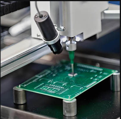
9-Solder Paste
The solder mask application is similar to the inner and outer layer processes. The main difference is that a photoimageable mask is used instead of photoresist over the entire surface of the production panel. The artwork is then used to take an image on the top and bottom layers. After exposure, the mask is stripped off in the imaged areas. The goal is to expose only the areas where components will be placed and soldered. The mask also limits the surface finish of the PCB to the exposed areas.
10-Surface Finish
There are several options for the final surface finish. Gold, Silver, 0SP, Lead Free Solder, Leaded Solder, etc. All of these are valid, but it really comes down to the design requirements. Gold and Silver are applied by electroplating, while Lead Free and Leaded Solder are applied by hot air solder level.
11-Nomenclature
Most PCBs are masked with markings on their surface. These markings are primarily used for the assembly process, with examples like reference markings and polarity markings. Other markings can be as simple as part number identification or a manufacturing date code.
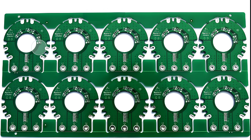
12-Depaneling
PCBs are produced in full production panels and need to be moved out of their manufacturing outline. Most PCBs are set up in arrays to increase assembly efficiency. These arrays can come in an infinite number of variations. Most arrays are either profile milled on a CNC milling machine using carbide tools or scored using diamond coated serrated tools. Both methods are effective and the choice of method is usually determined by the assembly team who will usually approve the arrays built in the early stages.
13-Testing
PCB manufacturers generally use either a flying probe or bed of nails testing process. The test method is determined by the number of products and/or available equipment.