What is chassis ground?Chassis ground is the metal chassis in the enclosure and establishes a connection to the chassis. Chassis ground is usually connected to earth at the point where power enters the power supply and can provide noise absorption or safety protection for parts of the system.
What are the types of PCB grounds?
Depending on the function and application, PCB grounds can be categorized into the following types:
Floating Ground: Floating ground occurs when a system does not have a reliable ground connection. The voltage of a floating ground is uncertain and may cause signal distortion or false triggering. In some cases, floating ground can be used to isolate different power sources or signals to increase safety or reduce interference.
Earth: This is the physical connection to the earth and is often used to draw residual current or provide a safe return point. The earth can effectively suppress external interference such as electrostatic discharge (ESD) or lightning strikes.
Chassis Ground (Safety Ground): This is the connection of a safety wire from the AC power source to the product enclosure or chassis, and is often used interchangeably with the term Safety Ground. Chassis grounding protects against hazards such as electric shock or fire, and provides a Faraday cage effect to shield against external noise.
Signal Ground: this is the reference point for any analog or digital signals used in a circuit and is usually the same as power ground. Signal ground ensures phase and amplitude consistency between signals and reduces the impedance of the signal loop.
Virtual Ground: This is a virtual ground point that is not directly connected to the actual ground path, but remains matched to the ground reference potential. Virtual ground is commonly used in analog circuits such as operational amplifiers to simplify circuit analysis and design.
AC Ground: This is a grounding point with a low impedance DC value that is stable even with small disturbances. AC grounding cannot be used as a suitable grounding point, but it can be used as a reference point. AC grounding is often used to bring grid power into circuit boards that require moderately high current operation.
Multi-point grounding: This is when wiring between two devices with a different ground point connected at each end. Multi-point grounding may result in a DC potential difference between the two grounding points, which can generate large DC currents or common mode noise.
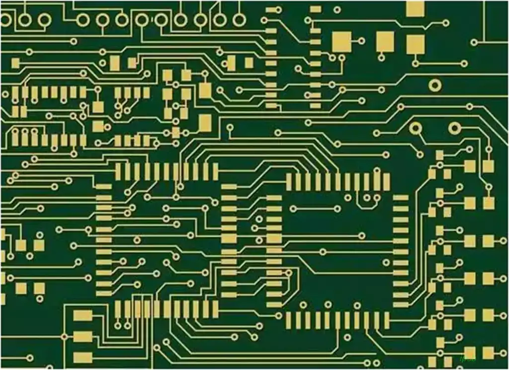
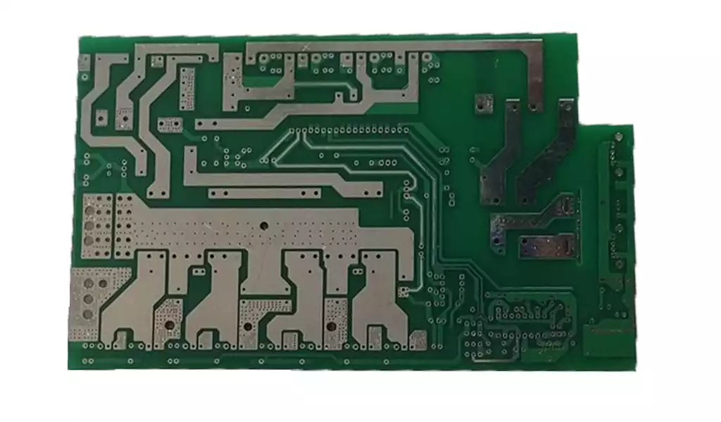
Importance of PCB Grounding Layer
Voltage Return
Voltage Return: Most components on a PCB are connected to the power grid and then the return voltage is returned through the ground grid. On boards with only one or two layers, the ground grid usually has to use wider wiring. However, by using an entire layer for the grounding layer in a multilayer board, it simplifies the process of connecting each component to the grounding grid.
Signal Return
Signal Returns: Regular signals also need to be returned, and for high-speed designs, it is important that they have a clear return path to the ground plane. Without this clear return path, these signals can cause a lot of interference to the rest of the PCB board.
Reducing Noise and Interference
Reducing noise and interference: As signal speed increases, more digital circuits switch states. This creates noise pulses in the grounding circuit that may affect the rest of the circuit. A ground plane with a large conductive area helps to minimize this interference because it has a lower impedance than the ground grid when it passes through the wiring conductors.
By carefully planning the layered stacking configuration of a multilayer board, PCB designers can use the grounding plane to help control the electrical performance of the board. By using a ground plane between two active signal layers, crosstalk between signals on those layers can be eliminated. Signal integrity of high-speed transmission lines can be improved by ensuring that there is an uninterrupted signal return path to the ground plane. Ground planes are also typically connected to heat-generating components to help dissipate heat.
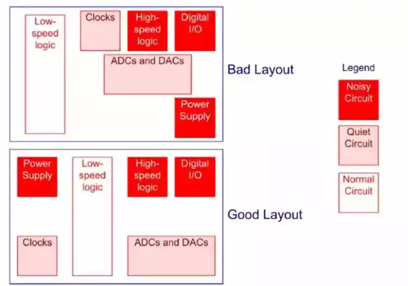
The design of the PCB ground plane requires the following considerations:
It should be located as close as possible to the signal line or component to minimize loop area and reduce impedance and noise.
It should be split as continuously as possible to avoid the formation of loops or islands that can lead to signal backflow or interference.
Should be layered and partitioned as much as possible to distinguish between different types or frequencies of signal ground, digital ground, analog ground, power ground, etc. to avoid mutual interference or crosstalk.
It should be oriented as parallel or perpendicular to the signal line as possible in order to reduce the crossing point or crossing angle, and to reduce the parasitic parameter and coupling effect.
Should try to keep a certain distance from the signal line to avoid excessive parasitic capacitance or inductive reactance affecting the signal quality.
Try to use a large grounding plane or grounding grid to improve the grounding effect and shielding effect.
In order to ensure the performance, stability and safety of electronic equipment, designers should fully understand the principle and application of chassis ground, and fully consider the grounding requirements in the design process. Through reasonable chassis grounding design, we can provide a stable and reliable working environment for electronic equipment to meet the needs of various complex application scenarios.