The laminated construction of PCB circuit boards refers to the stacking of multiple layers of circuit boards together to form a single structure. Electronic components can be arranged on each layer of the pcb circuit board, and the components are connected between the layers by means of wires and jacks. The laminated structure can provide a higher level of integration and more complex functionality.
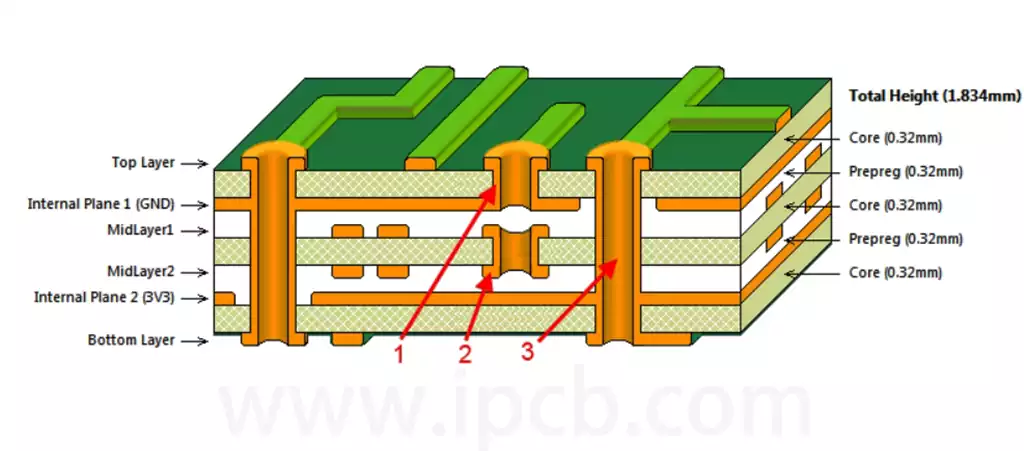
The PCB laminate structure consists mainly of a Core, which has two surface layers of copper foil with solid material filling between the layers, and a Prepreg (semi-solid sheet, or PP), which is a semi-solid resin that acts as a filler. Different Core and PP thicknesses can be selected to form a variety of laminated structures to suit different design requirements.
Each layer of the pcb circuit board in a stacked structure can be divided into different layers, usually including a top layer, an inner layer, and a bottom layer. The top layer is the most superficial layer of the pcb circuit board, on which most of the components and connecting wires are arranged. The internal layer is the circuit board placed between the top layer and the bottom layer, and can have multiple internal layers in which components are arranged that need to be connected to external signals. The bottom layer is the lowest layer of the circuit board, which is mainly used for mounting connectors and other external interfaces.
The design of a laminated structure requires the following key information in advance:
The total number of layers of the veneer, including the specific number of signal, power and ground layers.
The overall thickness of the veneer.
Target impedance values for single-ended and differential signals.
The dielectric constant (Er) of the material used for the PCB circuit board.
Determination of the number of veneer layers
At the beginning of the design process, the number of signal, power and ground layers should be estimated according to the veneer size, scale (e.g., number of signals, type of power supply, etc.), and electromagnetic compatibility (EMC) requirements, so as to determine the total number of layers of the veneer. The higher the number of layers, the more space for wiring and the better the EMC performance, but the corresponding cost will also increase. Usually the design process first component layout, through the PCB design software fly-by-wire display function, based on the density of the signal lines between the key devices to assess the number of signal layers required. After determining the signal layers, the number of power and ground layers are evaluated based on the type of power supply and the isolation requirements of the signal layers.
Veneer Thickness
Veneer thickness depends on a variety of factors such as the total number of layers. Generally, the thickness of the veneer can be 1.6mm for up to 12 layers; for more than 12 layers, it is recommended that the thickness be no less than 2mm.
Target Impedance
To ensure signal integrity, the signal transmission path requires impedance matching. Normally, the impedance of single-ended signal reference ground is set to 50 Ω, and the impedance between two lines of differential signal is 100 Ω. Some special applications have specific impedance requirements, such as USB differential impedance of 90 Ω, and some SOC chips may require 40 Ω or 45 Ω and other values.
PCB Material Selection
Dielectric Constant (Er): Reflects the ability of electromagnetic field conduction in the material. the larger the Er value, the stronger the material conductivity. In design, the commonly used FR4 material Er is generally between 3.5 and 4.5. High-speed circuit designs usually choose materials with smaller Er (e.g., 3.5 to 3.8) to reduce the loss of high-frequency signals.
Dielectric Loss Tangent (tan δ): Reflects the degree of signal loss in a material. the larger the tan δ value, the greater the signal loss. Unlike Er, tan δ is usually unaffected by frequency variations. High-speed PCB designs use materials with lower Er and tan δ to ensure signal integrity, although this can drive up the cost.
PP Sheet and Core Materials
PP (prepreg) and Core (core) are interlayer materials that come in different types corresponding to different thicknesses and copper foil specifications. The thickness of each model is mainly chosen based on the total board thickness and interlayer layout. For example, a thinner interlayer material will be designed between the power and ground layers, and a thicker one between the signal layers. Vendors usually provide detailed model specifications, including pcb circuit board thickness, interlayer thickness difference, and dielectric constant, for designers to use in impedance calculations and laminate structure design.
The basic principles of single pcb circuit board layer stack design are as follows:
(1) The second layer adjacent to the component side is the ground plane, which provides a device shield and a reference plane for the top wiring.
(2) All signal layers are adjacent to the ground plane as much as possible to ensure complete return paths.
(3) Avoid direct proximity of two signal layers to reduce crosstalk.
(4) The main power plane layer is adjacent to its corresponding ground plane as much as possible to form a plane capacitance and reduce the power plane impedance.
(5) Take into account the symmetry of the laminated structure, which is conducive to PCB circuit board production warpage control. The above are the conventional principles of laminated design, in the actual implementation of laminated design, PCB engineers in the adjacent wiring layer by increasing the spacing, reducing the distance from the corresponding wiring layer to the reference plane, and then control the interlayer wiring crosstalk under the premise that the two signal layers can be directly adjacent to each other. For more concerned about the cost of consumer electronics products, you can weaken the power plane and ground plane adjacent to reduce the plane impedance of the way, so as to minimise the wiring layer, reduce PCB circuit board costs. Of course, there is a certain risk of doing so. For backplane stacking design, due to the common backplane is difficult to do neighbouring lines perpendicular to each other, so there will inevitably be parallel long-distance wiring.
For high-speed backplane, the general principles of stacking are as follows:
(1) TOP surface, BOTTOM surface for the complete ground plane, constituting a shielding cavity.
(2) No neighbouring layers are wired in parallel to reduce crosstalk; or the spacing between adjacent wiring layers is much larger than the reference plane spacing.
(3) All signal layers are adjacent to the ground plane as much as possible to ensure a complete return channel. It should be noted that, in the specific PCB stacking setup, to flexibly apply the above principles, according to the actual needs of the veneer, and ultimately determine the appropriate layer stacking scheme, do not copy the rigid set.
Optimising the PCB circuit board layer stacking structure to meet the electromagnetic compatibility (EMC) and signal integrity is a key step in the actual design, mainly through the rational arrangement of the signal, power and ground layers of the location, selecting the appropriate materials, and the use of simulation tools to verify the design.
Reasonable Arrangement of Layered Structure Layout
Signal Layers Adjacent to Reference Layers: Each signal layer should be adjacent to a complete reference layer (power or ground layer) to provide a low impedance return path, reduce electromagnetic radiation and crosstalk, and help improve signal integrity and EMC performance.
Power and ground layers are tightly coupled: the ground layer is generally placed above the power layer, and the interlayer medium is as thin as possible, so that the interlayer capacitance formed is conducive to decoupling the power supply, reducing power supply noise, lowering impedance, and effectively suppressing common mode interference.
Avoid neighbouring signal layers directly adjacent to each other: it is best to separate at least one power or ground layer between two signal layers, so as to avoid direct coupling between signals, reduce crosstalk and improve signal quality.
High-speed signal layer sandwiched between two internal electrical layers: High-speed differential signals should be placed between two ground layers to form a strip line (Stripline) structure, shielding interference, ensuring impedance matching, reducing signal reflection and crosstalk.
Symmetric stacked layer design: the stacked structure should be as symmetric as possible, which is conducive to the uniform distribution of thermal stress, reduce the risk of board warping, improve manufacturing yields and board reliability.
Layer stacking structure design is the key to the performance of the PCB circuit board, a reasonable layer stacking scheme not only improves the signal integrity and electromagnetic compatibility, but also effectively control the cost and manufacturing difficulties. In the future, as the demand for high-speed and high-density design continues to rise, the optimisation of the laminated structure will continue to be a core issue in PCB design, promoting the development of electronic products to a higher level.