PCB Copper Layup is the process of filling areas of a PCB board that are not wired or unused spaces with solid copper skins.
Copper plays multiple key roles in PCB design including, but not limited to, reducing ground impedance, enhancing interference immunity, connecting to ground to reduce loop area, and promoting heat dissipation.
Copper is effective in reducing ground impedance and providing shielding and noise suppression. In digital circuits, it is particularly important to reduce ground impedance due to the presence of large amounts of spiked pulse currents. Laying copper by expanding the conductive area of the ground line, shorten the length of the ground line to reduce inductance, as well as appropriate control of the ground line capacitance to improve the conductivity, thus achieving the purpose of reducing the ground line impedance. Large-area ground or power supply copper can also play a role in electromagnetic shielding, reduce electromagnetic interference, enhance the circuit’s anti-interference ability to ensure that meet the electromagnetic compatibility (EMC) requirements. For high-frequency circuits, laying copper for high-frequency digital signals to provide a complete return path, reducing the wiring of the DC network, thereby enhancing the stability and reliability of signal transmission.
Copper laying also plays the role of heat dissipation in PCB design. As the metal has good electrical and thermal conductivity, copper paving increases the PCB board internal gap and other blank areas of the metal composition, thereby increasing the surface area of the heat dissipation, which helps the overall heat dissipation.
Copper paving can also help to evenly distribute heat to avoid local high temperature areas, by evenly distributing heat to the entire PCB board, reducing local heat concentration, reducing the temperature gradient of the heat source, and improving the efficiency of heat dissipation. In PCB design, the use of copper can be used to dissipate heat in a number of ways, including: according to the distribution of heat source reasonable design of the heat dissipation area and lay enough copper foil, increase the thickness of the copper foil to increase the thermal conductivity of the path, the design of the heat dissipation through the holes in order to heat conduction to the other side of the PCB board, as well as in the area of heat dissipation by adding a heatsink, through the natural convection or fan cooling and other ways to improve the efficiency of the heat dissipation.
Copper paving also reduces deformation and improves the manufacturing quality of the PCB board.Copper paving helps ensure uniformity of plating and reduces board deformation during lamination, which can significantly improve manufacturing quality, especially for double-sided or multi-layer PCB board. Copper spreading can effectively reduce the problem of uneven distribution of copper foils, so that the whole board is more evenly distributed.
Copper paving also meets the mounting requirements of special devices. For some devices that need to be grounded or have special installation requirements, copper paving can provide additional connection points and fixed support to enhance the stability and reliability of the device.
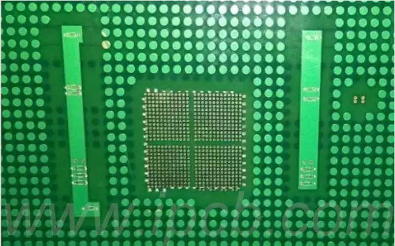
There are two main forms of PCB copper-laying technology: solid copper-laying and grid copper-laying, each of which has its own unique characteristics and application scenarios.
1.Solid copper paving is able to enhance the current-carrying capacity and has excellent shielding performance. However, when passing through the wave soldering process, the solid-laid copper will have a certain tensile force due to thermal expansion and contraction effect, which may lead to warping of the board and even the generation of air bubbles. In order to mitigate the adverse effects of this tension on the copper foil, it is common to design a few slots in the solid-laid copper.

2.Grid-laying copper, on the other hand, is mainly used for shielding as its main function, and its ability to enhance current is relatively weak. From the point of view of heat dissipation, the grid copper design not only reduces the direct heat area of copper, but also maintains the effect of electromagnetic shielding. However, it is worth noting that the production process has specific requirements for the shape of the copper grid, if the grid design is too small, it may have a negative impact on the quality of the product yield.
The Importance of Copper Pitch and Wire Pitch in PCB Board Design
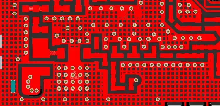
Copper pitch, the vertical distance between neighbouring copper layers on a pcb board, has a significant impact on the pcb board’s thermal, electrical and mechanical properties. If this pitch is too large, the thermal conductivity of the circuit board will be weakened, affecting heat dissipation; if too small, it may increase the interlayer capacitance, resulting in signal interference. Therefore, in the design, according to the actual needs of the circuit board and the manufacturing process, a reasonable set of copper spacing.
Wiring spacing, is the horizontal distance between adjacent wires on the circuit board, also has an important impact on the performance of the circuit board. Reasonable spacing can effectively reduce the crosstalk between the wires and signal interference, improve the stability and reliability of signal transmission.At the same time, the setting of the wiring spacing also need to take into account the cost of manufacturing circuit boards and process difficulties.
Too small a distance may increase the cost, while too large a waste of circuit board space.
In the design of copper spacing and wiring spacing, engineers need to consider a number of factors. The first consideration is the actual needs of the board, including operating frequency, signal transmission speed, heat dissipation requirements. Secondly, the limitations of the manufacturing process should not be ignored, different processes on the pitch requirements may vary.In addition,the reliability of the circuit board and cost and other factors also need to be taken into account.
Conventional standards for copper laying and wire spacing:
In general,in order to ensure the reliability and efficiency of the pcb board,the copper and wire spacing should not be less than 0.2 mm, this standard is based on industry norms and practical design experience,applicable to most standard circuit board design.
For high-speed transmission pcb boards or high-frequency signal circuit boards,due to the faster signal transmission rate,the spacing requirements are more stringent.The copper and wire spacing on such boards usually needs to be maintained at 0.25-0.3mm or more to effectively reduce signal interference and improve transmission efficiency.
For some high-end electronic products, such as the use of blind holes in the design of flexible circuit boards (FPC boards), etc., laying copper and wire spacing requirements are even more precise. The spacing of such products usually needs to reach 0.15-0.25mm or more to ensure higher manufacturing precision and reliability.
PCB copper laying technology through the fine design, significantly improve the overall performance and manufacturing quality of the pcb board. Whether it is to reduce ground impedance, enhance heat dissipation, or to improve anti-interference capability, copper paving plays an indispensable role. In the future, with the continuous progress of technology, copper-laying technology will continue to contribute to the development of electronic products.