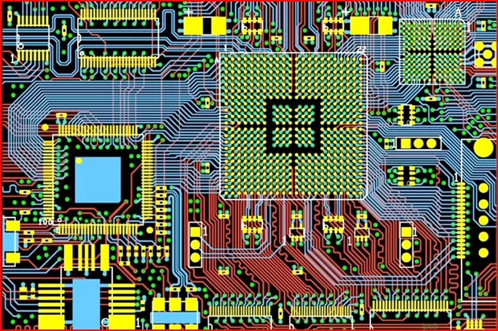
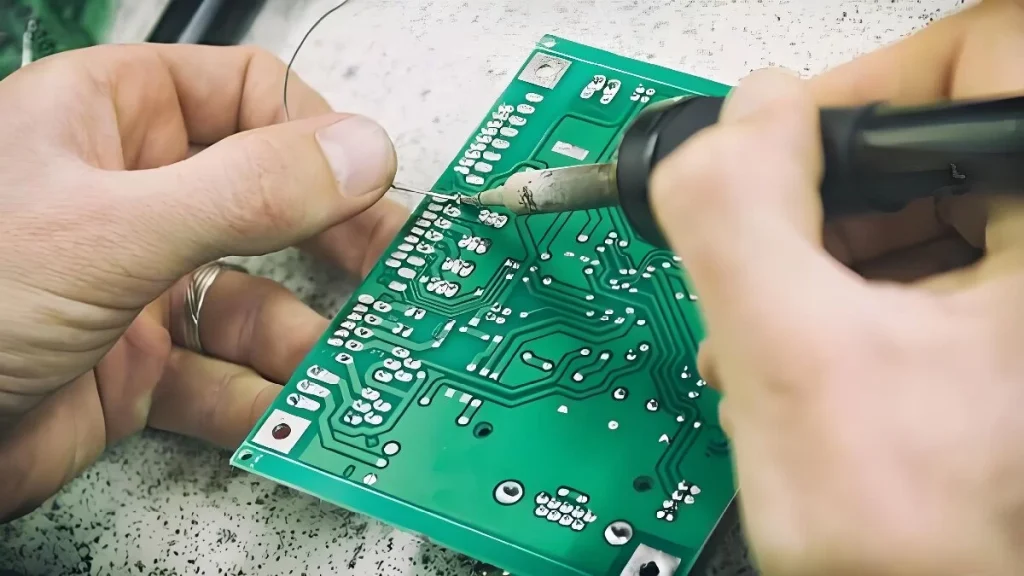
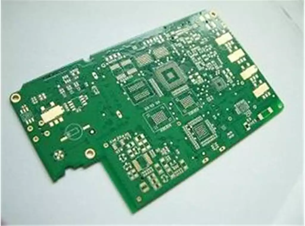
PCB voltage clearance, usually refers to the minimum distance between different conductive parts of the PCB (such as alignments, pads, vias, etc.). This distance is to prevent electrical short circuits and ensure electrical insulation and set up, and is affected by a variety of factors, including PCB operating voltage, dielectric strength of the insulating material, ambient temperature and humidity. The shortest path between two electrically conductive parts or between an electrically conductive part and the protective interface of the equipment, measured along the insulating surface. That is, in different use cases, due to the conductor around the insulating material is electrodeposited, resulting in the insulating material presents a charged phenomenon is the creepage distance.
Electrical clearance requirements
The distance can be determined according to the measured operating voltage and insulation level.
Primary side AC part: L-N ≥ 2.5mm before the fuse, L.N-PE (earth) ≥ 2.5mm, after the fuse device may not be required, but as far as possible to maintain a certain distance in order to avoid short-circuit damage to the power supply.
AC to DC part of primary side ≥2.0mm.
Primary side DC ground to earth ≥2.5mm (primary side floating ground to earth).
Primary side AC to secondary side ≥4.0mm, across the components between the primary and secondary sides.
The gap clearance of the secondary side is ≥0.5mm.
Secondary side ground to earth ≥ 1.0mm can be.
Creepage distance requirements
Primary side AC part: L-N before the fuse ≥ 2.5mm, L.N-earth ≥ 2.5mm, after the fuse may not be required, but try to maintain a certain distance to avoid short-circuit damage to the power supply.
AC to DC part of primary side ≥2.0mm.
Primary side DC ground to earth ≥ 4.0mm, such as primary side ground to earth.
Primary side of the secondary side ≥ 6.4mm, such as optocouplers, Y capacitors and other parts of the Yuan apparatus foot spacing ≤ 6.4mm to slot.
Between the secondary side of the part ≥ 0.5mm can be.
Secondary side ground to earth ≥ 2.0mm or more.
Transformer between two levels ≥ 8.0mm or more.

Steps for selecting creepage distance and creepage clearance
1. Determine the steps of electrical clearance
Determine the peak and RMS values of the operating voltage;
Determine the supply voltage of the equipment and the category of the supply facility;
Determine the size of the transient overvoltage entering the equipment according to the overvoltage category;
Determine the pollution level of the equipment (generally pollution level 2 for equipment);
Determine the type of insulation across the electrical gap (functional insulation, basic insulation, additional insulation, reinforced insulation).
2. Determine the creepage distance steps
Determine the RMS or DC value of the operating voltage;
Determine the material group (according to compared to the leakage trace index, which is divided into: Ⅰ group materials, Ⅱ group materials, Ⅲa group materials, Ⅲb group materials. Note: If the material group is not known, it is assumed that the material is group Ⅲb)
Determine the pollution level;
Determine the type of insulation (functional insulation, basic insulation, additional insulation, reinforced insulation).
3. Determine the required value of electrical clearance
According to the measured operating voltage and insulation level, check the table (GB4943-2011 “Safety of Information Technology Equipment”: 2H and 2J and 2K, 60065-2001 table: Table 8 and Table 9 and Table 10) Retrieve the required electrical clearance can determine the distance; as an alternative to the electrical clearance, 4943 use Appendix G to replace, and 60065-2001 use Appendix J to replace.
GB 8898-2001: the main factor considered for electrical clearance is the operating voltage, check Figure 9 to determine. (For and voltage RMS in the 220-250V range of grid power conductive connection parts, these values are equal to the peak voltage of 354V corresponding to those values: basic insulation 3.0mm, 6.0mm reinforced insulation)
4. Determine the creepage distance requirement value
According to the operating voltage, insulation level and material group, check the table (GB 4943 for Table 2L, 65-2001 for Table 11) to determine the creepage distance value, such as the operating voltage value in the table between the two voltage ranges, you need to use the internal difference method to calculate the creepage distance.
GB 8898-2001 its determination of the value is equal to the electrical clearance, such as to meet the following three conditions, the electrical clearance and creepage distance reinforced insulation can be reduced by 2mm, the basic insulation can be reduced by 1mm:
(1) These creepage distance and electrical clearance will be reduced by external forces, but they are not in the shell of the accessible conductive parts and dangerous charged parts between;
(2) They remain unchanged by a rigid structure;
(3) Their insulation characteristics will not be seriously affected by the dust generated inside the equipment.
The spacing of the alignment: according to the PCB board manufacturer’s processing capabilities, between the wire and the wire, the wire to the pad between the spacing should not be less than 4 mil. usually, in order to meet the production needs of the general conventional spacing of about 10 mil.
The width of the alignment: the width of the alignment should be determined by the size of the current. For example, when the copper thickness of 1OZ, 1mm line width can be taken by the current 1A to take the value of the conditions allow, the alignment should be as wide as possible in order to reduce resistance and improve reliability.
When designing PCBs, it should be ensured that the creepage distance is large enough to prevent leakage or breakdown under high voltage or harsh environmental conditions. This usually means that a wider insulating area between conductive sections or the use of insulating materials with higher arc resistance is required.
1. During the design process, minimize the length and curvature of the line to reduce resistance and inductance.
2. Whenever possible, wide conductors and large spacing should be used to improve reliability.
3. Avoid crossing or overlapping wires to prevent electromagnetic interference and thermal effects.
4. Where high frequency signal transmission is required, shielded cable or fiber optic transmission should be used to reduce interference.
5. In cases where high current transmission is required, thicker wires should be used to reduce resistance.
6. Where mechanical stresses may occur, appropriate outer jackets should be used to protect the conductors.
7. Maintainability of the circuit should be considered during the design process to facilitate maintenance and replacement of pcb components.
PCB voltage clearance and creepage distance are key parameters to ensure the electrical performance and safety of PCB. In the design process,it is necessary to set these two parameters according to the circuit’s operating voltage, insulation requirements, environmental conditions and production processes and other factors to be reasonable. Through reasonable clearance and creepage distance design, can significantly improve the reliability and service life of PCB.


