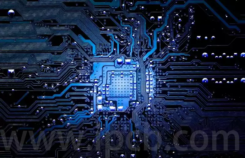
PCB etching is the process of removing unwanted copper (cu) from a circuit board. When it is not needed, it is simply non-circuit copper that is removed from the board based on the PCB design and the desired circuit pattern is obtained.
In other words, etching is like chiseling a circuit board; let’s say the board is a rock and etching chisels the rock into a beautiful sculpture. In this process, the substrate copper or starting copper is removed from the board, and both rolled and annealed copper are easier to etch off than electroplated copper.
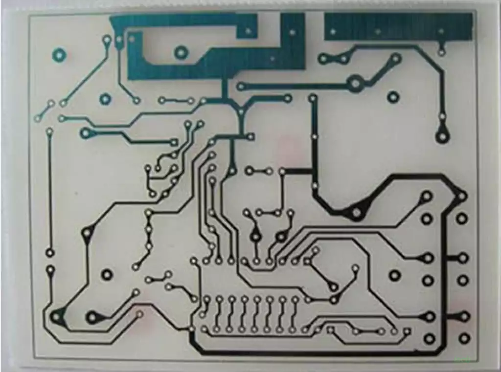
How to etch a pcb board
Depaneling, the depaneling solution in the machine will remove the dry film that has been exposed on the board, the dry film on the board disappears to reveal the copper, but this copper is not what we need, we need the copper is under the tin, and then the board enters into the etching process, the chemical solution only reacts to the copper and does not affect the tin, so the exposed copper will be etched away, the inner layer of the multilayer boards and the single and double boards of the outer layer, according to the requirements and process characteristics of the acid or alkaline can be selected characteristics to choose acidic or alkaline corrosion solution.
In general, the inner layer is more suitable for acidic etching solution, while the outer layer is more suitable for alkaline etching solution. After the etching, the line on the board is only tin (tin needs to be removed), the board will move with the roller into the de-tinning section, where a chemical solution will be used to dissolve the tin layer on the circuit board, so that the line back to the original color of copper.
After the etching process is over it will go to the next process – AOI inspection, the circuit board will be placed in a special inspection equipment, the use of ultra-high-definition optical cameras and graphic processing systems to scan the surface of the PCB, to obtain high-definition images for analysis and comparison, to detect possible defects and problems, and to correct and optimize the. After determining the good product, it will go to the next process — solder resist.
PCB board etching process considerations
Uniformity of the line
PCB prototyping circuit boards generally need to go through the etching process. For example, the full-plate copper-plating process needs to be etched off the photographic film outside the part, but in the etching operation must also maintain the uniformity of the line, while the board surface of the various parts of the plate should be plated twice copper, but also need to etch off the periphery of the panel, so as to maintain the uniformity of its lines and panels with the reliability of the panel.
Suitable etchant
The vast majority of multilayer circuit boards in the etching operation, are based on sulfate etching solution, in which the copper is separated by electrolysis. PCB multilayer circuit boards in the etching process, in which the copper is generally separated by electrolysis, only the right corrosive agent can be reused, so etching operations must be to choose the right corrosive agent.
Etching speed
PCB multilayer circuit board etching process also requires reasonable control of the corrosion rate of the corrosive agent. Today’s market commonly used corrosives are water/ammonia chloride etching solution, in the use of reasonable corrosion rate is also needed, because the corrosion rate is too fast may lead to the PCB board board are experiencing corrosion, while the corrosion rate is too slow may lead to poor corrosion of its board.
Types of etching PCB
Graphic plating method: etching when the board has two layers of copper, only one layer of copper is all etched off, the rest will form the final required circuit.
Full-plate copper plating process: the entire board is plated with copper, the part outside the photographic film is only tin or lead-tin resist layer. Compared with the graphic plating, its biggest disadvantage is that all parts of the board have to be plated with copper twice, and they must all be etched away when etching.
There is another method, which is to use a photographic film instead of metal plating as a resist layer. This method approximates the inner layer etching process.
Etchant
Ammonia-based etchants are commonly used chemical fluids that do not have any chemical reaction with tin or lead-tin. In addition, there are ammonia/ammonia sulfate etchant solutions, which, when used, contain copper that can be separated by electrolysis; they are generally used in chlorine-free etching. Others use sulfuric acid – hydrogen peroxide as an etchant to etch the outer layer of graphics, has not yet been adopted in large quantities.
Factors affecting the characteristics of the etching solution
(1) the concentration of etching solution: should be based on the principle of metal corrosion and the type of structure of copper foil, through the test method to determine the concentration of etching solution, it should have a greater choice, which means that the process range is wider.
(2) the composition of the chemical composition of the etching solution: the chemical components of the etching solution is different, its etching rate is not the same, the etching coefficient is also different. Such as the general use of acidic copper chloride etching solution etching coefficient is usually &; alkaline copper chloride etching solution coefficient up to 3.5-4. And is in the development stage of the nitric acid-based etching solution can be achieved almost no side corrosion problems, etched wire sidewalls close to vertical.
(3) temperature: temperature on the characteristics of the etching solution has a relatively large impact, usually in the chemical reaction process, the temperature to accelerate the fluidity of the solution and reduce the viscosity of the etching solution to improve the etching rate plays a very important role. But the temperature is too high, but also easy to cause some of the chemical components in the etching solution volatilization, resulting in the chemical composition of the etching solution in the proportion of imbalance, and at the same time, the temperature is too high, may cause the polymer antioxidant layer is destroyed and affect the etching rate.
Etching layer is destroyed and affect the service life of etching equipment. Therefore, the etching solution temperature is generally controlled within a certain process range.
(4) The thickness of the copper foil used: the thickness of the copper foil has an important impact on the circuit pattern of the wire density. Thin copper foil, etching time is short, side corrosion is very small; conversely, side corrosion is very large. Therefore, the copper foil thickness must be selected according to the technical requirements of the design and the circuit pattern of the wire density and wire precision requirements. At the same time the copper elongation, surface crystallization structure, etc., will constitute a direct impact on the characteristics of the etching solution.
(5) The geometry of the circuit: circuit pattern wire in the X direction and Y direction of the distribution of the position if the imbalance, will directly affect the etching fluid flow rate on the board. Similarly if the same board on the narrowly spaced wire parts and widely spaced wire parts state, widely spaced wire distribution parts, etching will be excessive. Therefore, this requires the designer in the circuit design, it should be the first to understand the feasibility of the process, as far as possible to achieve a uniform distribution of circuit graphics across the board, the thickness of the wire should be as consistent as possible. Especially in the production of multi-layer printed circuit boards, large areas of copper foil as a ground layer, the quality of etching has a great impact, so it is recommended that the design into a mesh pattern is appropriate.
PCB etching process as a key link in the manufacture of circuit boards, the degree of fineness is directly related to the performance and quality of the circuit board. Starting from the design of the circuit diagram, to the final assembly test, each step needs to be strictly controlled to ensure that the etched circuit pattern meets the design requirements.