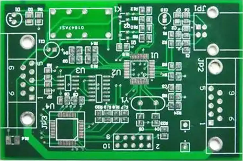
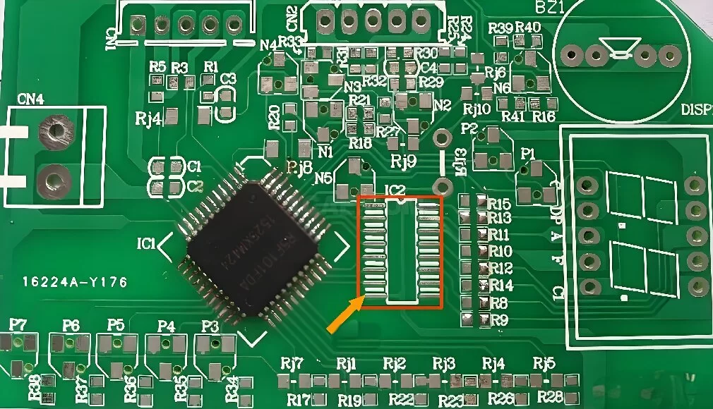
Printed Circuit Board fiducial marks are a reference point or identifier used to determine the relative position of other components or features on a PCB. These markers play a vital role in the manufacturing, testing, and assembly processes to ensure that components are accurately placed in the correct location for proper functioning of the circuit board.
Fiducial marks are often designed as specific graphics or identifiers so that they can be easily identified and positioned during the manufacturing process. They may include markings etched into the surface of the PCB, metallized through-holes, or other forms of identifiers. These markers are usually located at the corners or edges of the circuit board so that they can be easily located by both automated equipment and manual labor.
What are the types of PCB Fiducial marks?
There are two main types of PCB reference marks. This relates to their location and position on the printed circuit board.
Local datum markings
Local datum PCB markings are necessary to locate the position of each component. This occurs when the component requires a higher degree of precision.
Global Datum Markers
Global datum PCB markers are manufactured to help differentiate between the panel datum and the circuit pattern of the PCB. The location can be accomplished relative to a grid system with three points. The lower left datum is located at the origin (0,0), while the remaining two are located on the positive axes x and y. If more than one board needs to be processed at the same time, they are referred to as panel datums.

Best Practices for Using Benchmark Markers in PCB Designs
If you want to get the best out of your machine assembly, you need to get the right benchmark pcb markers. There are few important guiding principles when it comes to placing a reference mark in a design.
Benchmarks are made by placing an undrilled copper layer in a circle. The datum mark must not have a solder mask.
The optimum size of the datum mark should be between 1mm and 3mm. A clearance area similar to the diameter of the mark must be maintained.
For the global reference point, 3 markers are placed at the edge of the board for best accuracy. In case of lack of space, at least one global reference pcb mark is required.
The reference mark must be placed 0.3 inches from the board edge, excluding the clearance area for the fiducial marks.
For localized datums, place at least two datum markers diagonally across the outer edges of surface mount components.
PCB manufacturers are using specialized PCB design software, such as Altium’s CircuitStudio®, which inserts pads, changes the pad size to zero, and sets the correct diameter value for placing the datum PCB markers.
By using fiducial marks, manufacturers can ensure that components on the PCB are placed with the required accuracy, thereby improving product reliability and performance. The datum markers can also be used to calibrate test equipment during the test phase to ensure the accuracy of test results.


