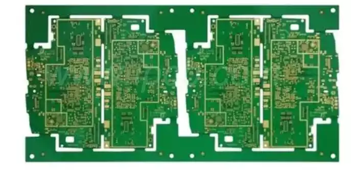
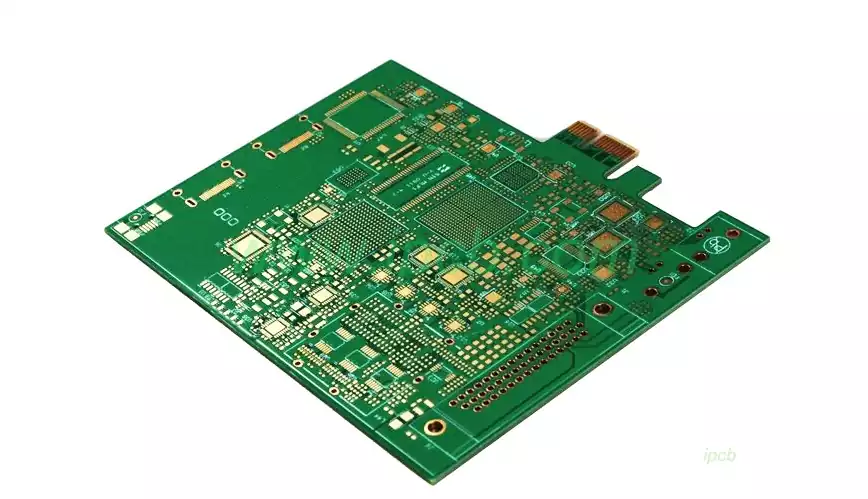
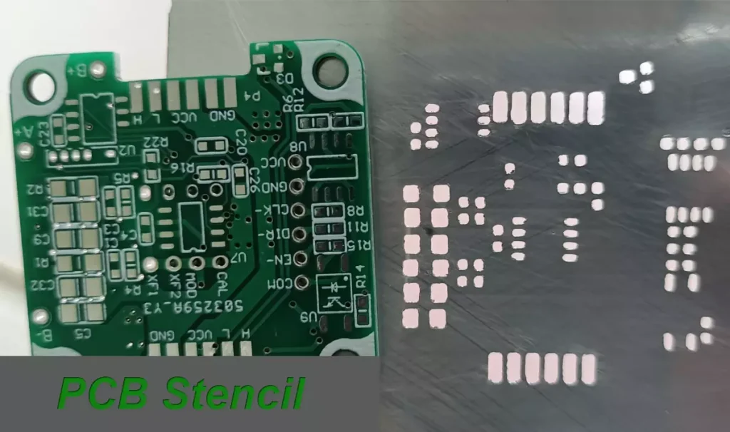
The pcb hole size is usually determined by the design requirements and application. In general, the size of the hole depends on the required current capacity and the size of the component pins. Larger mounting holes can withstand higher currents, but also take up more board area. Designers only usually refer to standard sizes and specifications, such as the IPC standard, to select the appropriate via size. Typically, the aperture size should be greater than or equal to the diameter of the pin or resistor plus twice the machining tolerance.
PCB aperture standards are developed by the International Electrotechnical Commission (IEC), which is commonly referred to as the IPC standard. ipc-2222 and ipc-2221 are currently the most commonly used standards, which specify the layout,size,aperture, and other relevant parameters of various components in PCB design.
According to IPC standards, PCB apertures are categorized into two types:
Mechanical apertures and electrical apertures. Mechanical apertures are holes for mounting components or connecting wiring.
Electrical aperture refers to the hole used to lead out the electrical signal. In practice, we often need to choose the right aperture according to the specific design requirements.
Standard Dimensions for Printed Circuit Board Drilling
The standard sizes for printed circuit board drilling are usually measured in inches or millimeters, with common sizes such as 0.3mm, 0.4mm, 0.5mm, 0.6mm, 0.7mm, 0.8mm, 0.9mm, 1.0mm, 1.2mm, 1.5mm, 1.8mm, and 2.0mm.Among them,0.3mm, 0.4mm, 0.5mm and 0.6mm are the conventional drilling sizes for most of the PCB manufacturing requirements.
Manufacturing requirements for PCB drilling
- The location and size of the drilled holes should be in accordance with the design requirements,and the tolerance of the hole diameter should be controlled within ± 0.05mm;
- The drilled holes should not produce burrs or welding film and other issues,if necessary,should be dealt with accordingly;
- The drilled holes should have good roundness and surface quality,and should not produce deformation or cracking and other problems;
- The depth of the drilled holes should meet the design requirements and should be adjusted accordingly if necessary.

Determinants of pcb hole size
Current demand: Larger currents require larger via holes to minimize resistance and thermal effects.
Number of layers on the board: Thicker boards may require larger vias to ensure complete penetration.
Material type: Different board materials have different conductivity and thicknesses,which can affect the size of the vias.
Manufacturing Capability: The manufacturer’s process capability will also limit the minimum size of the vias.
Design rules: Each PCB design project has a unique set of design rules,which may specify the minimum and maximum size of the vias.
Choosing the right PCB hole size main considerations.
Aperture diameter and lead diameter relationship: for PCB circuit board metallization holes, the use of round leads, the aperture diameter is generally larger than the lead diameter of 0.2mm (8mil) ~ 0.6mm (24mil),the specific size of the board thickness according to the election The specific size is selected according to the thickness of the board,the thicker the larger value,the thinner the smaller value.For board thickness in 1.6mm (63mil) ~ 2.0mm (79mil) of the board, the aperture diameter than the lead diameter is generally larger than 0.2mm (8mil) ~ 0.4mm (16mil).For lead diameter greater than 0.8mm (32mil),the board thickness of more than 2mm mounting holes, the gap should be appropriately large,you can take the larger 0.4mm ~ 0.6mm.
Over-hole size and design requirements: the size of the over-hole is usually determined by the design requirements and applications.Generally the value of the outer diameter minus the inner diameter (R outer diameter-r inner diameter) >= 8 mil (0.2mm).PCB through holes are available in diameters as small as 0.15mm, compared to the common size of 0.6mm. General recommendations for the outer diameter of 1MM, inner diameter of 0.3-0.5MM, for more dense lines, the outer diameter to 0.6MM,inner diameter to 0.4-0.2MM like.
The number and type of holes: the number of holes in the same design should not be too many,generally no more than 3 kinds.Conventional hole size of 8/16, 10/22, 12/24, under special circumstances can choose 8/14, 10/20, 10/18 type of hole For HDI design, 4/10 and 4/8 laser vias are generally used. Priority is given to the selection of large aperture type, which can improve the production of qualified rate and reduce production costs.
High speed PCB through hole design
Through the analysis of the parasitic characteristics of the over-hole, we can see that in high-speed PCB design, seemingly simple over-hole often also brings a great deal of negative effects on the design of the circuit. In order to minimize the negative impact of the parasitic effect of the over-hole, you can try to do in the design:
- From the cost and signal quality considerations, choose a reasonable size of the over-hole size. For example, for 6-10 layers of memory module PCB design, the choice of 10/20Mil (drilled holes / pads) over-hole is better, for some high-density small-sized boards, you can also try to use 8/18Mil over-hole. Under the current technical conditions, it is difficult to use smaller sized vias. For the power or ground over-hole can be considered to use a larger size to reduce impedance.
- PCB board signal alignment as far as possible without changing layers, that is to say, try not to use unnecessary holes.
- Power and ground pins should be played near the hole, the shorter the lead between the hole and the pin, the better, because they will lead to an increase in inductance. At the same time, the power and ground leads should be as thick as possible to reduce impedance.
- Place some grounded vias near the vias of the signal transitions in order to provide the nearest loop for the signals. It is even possible to place some extra grounded vias in large numbers on the PCB. Of course, there is still a need for flexibility in the design.
The vias discussed above are modeled as pads on each layer, but sometimes we can reduce or even remove the pads on certain layers. Especially in the case of a very high density of over-hole, may lead to the formation of a copper layer in the circuit to isolate the broken groove, to solve such a problem in addition to moving the location of the over-hole, we can also consider over-hole in the copper layer of the pad to reduce the size.
In PCB design, the pcb hole size is a balance between performance and cost.Accurate control of the hole size and optimize the layout is the key to ensure the performance and cost-effectiveness of high-speed circuits.


