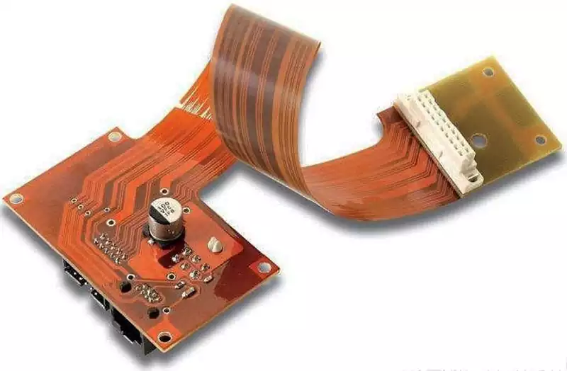
PCB lamination is a key process step in the manufacture of multilayer printed circuit boards (PCBs). In this process, multiple thin, pre-processed circuit board layers (including copper foils, insulating substrates, leadframes, etc.) are tightly bonded together under high temperature and pressure with a specific adhesive (usually epoxy) to form a monolithic multilayer structure.
The purpose of pcb lamination is to create a PCB with complex circuit layouts and interconnection structures that are electrically connected between the different circuit layers by means of via holes (e.g. plated through holes, blind holes or buried holes). This multilayer structure not only improves the electrical properties of the board, but also increases its mechanical strength and thermal stability.
Lamination is the core step in the manufacture of multilayer PCBs and is designed to tightly bond the layers of circuit boards into a solid whole with the help of specific techniques. The process is subdivided into three stages: kiss pressing, full pressing and cool pressing. In the kiss-pressing stage, the resin penetrates the bonding interface and fills in the tiny gaps in the circuitry; this is followed by the full press stage, which ensures that all gaps are completely sealed and bonded. The cooling press stage focuses on rapidly reducing the board temperature to maintain its dimensional stability.
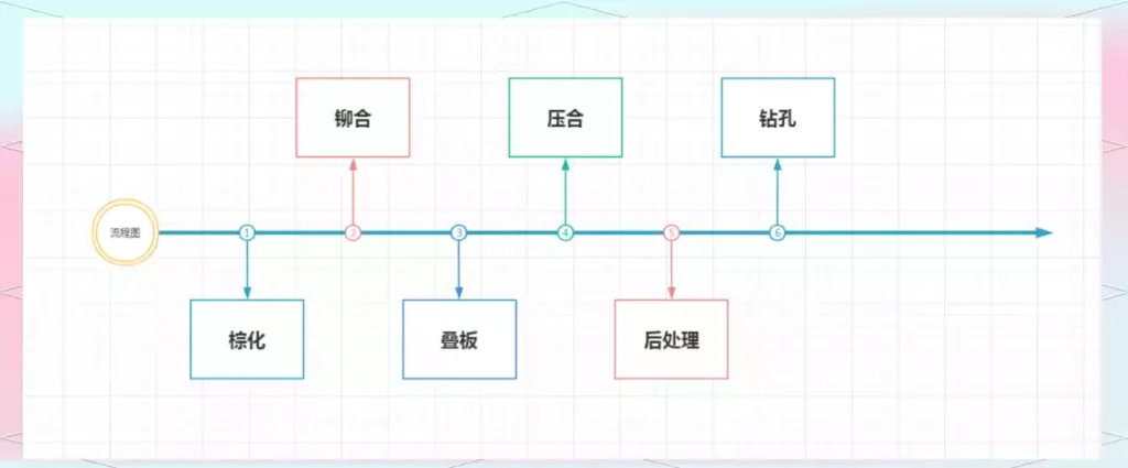
In addition, the browning process plays a crucial role in the preparation of the inner core. The browning process covers the copper surface with a homogeneous brown organometallic film, which not only strengthens the adhesion between the copper surface and the semi-cured material, but also prevents the chemical reaction between the copper and the amines in the semi-cured material during the high-temperature lamination process. The basic principle of the browning process involves the use of chemicals and equipment designed to roughen the copper surface, increase the surface area in contact with the resin, improve the wetting ability of the copper surface to the liquid resin, and passivate the copper surface to prevent unfavourable reactions from occurring. The main production raw material used in this process is the browning solution MS100, but it is worth noting that as the browning film is extremely thin and fragile, it must be handled with extreme care to prevent abrasion.
Riveting
Purpose: The main purpose of riveting in the manufacture of four-layer boards is to prevent possible displacements between the layers in subsequent processing steps by connecting the inner layers of the board tightly and securely together with the aid of rivets.
The core production materials are rivets and semi-cured sheets (P/P). The P/P is made by combining resin and glass fibre cloth through a special process. There are different types of glass fibre cloth, such as 101033132116 and 7628, which have a direct impact on the overall performance of the P/P.
Stacking Sheets
Objective: To stack sheets that have been pre-assembled into a multilayer sheet form ready for pressing.
Core Result: In the stacking process, copper foils, semi-cured sheets and electroplated copper skins are the key materials used.
The thickness of the copper foil generally consists of the following standard sizes:
1/3 ounce (OZ), which corresponds to a thickness of 12 microns (um) and is labelled T;
1/2 ounce (OZ), which corresponds to a thickness of 18 microns (um) and is labelled H;
1 ounce (OZ), which has a thickness of 35 microns (um) and is labelled 1;
and 2 ounces (OZ) with a thickness of 70 microns (um), labelled 2.
The selection of different thicknesses of copper foils has a direct impact on the performance of the final product.
Lamination
Objective: To press pre-stacked sheets into a multilayer structure by means of a hot pressing process.
In the pcb lamination process, the most important auxiliary materials include kraft paper and steel plates. The kraft paper acts as a barrier and protection, while the steel plate applies the necessary pressure to ensure that the sheets are firmly bonded together to create a solid multi-layer construction.
Post-treatment
Objective: At the end of the lamination process, edge grinding, perforating (or targeting), and edge milling operations are performed to give the sheet an initial profile to ensure that it meets the quality control standards of the subsequent production stages, and to prepare the necessary locating holes or tooling holes for the next processing steps.
Core production tools include drills and milling cutters, which play a vital role in this process.
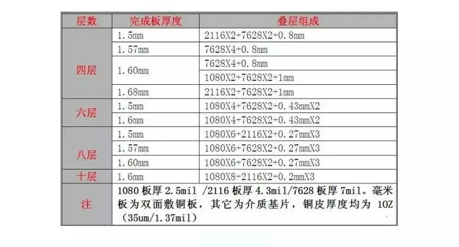
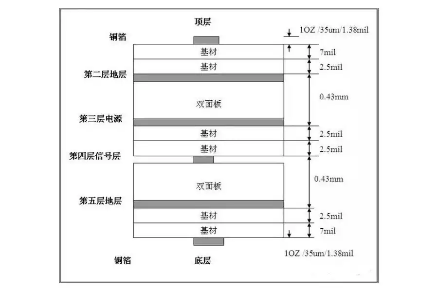
The lamination process and layering criteria for PCB boards are governed by the physical properties of the PCB boards, which include key parameters such as the total thickness of the multilayer PCB boards and the number of layers. Given the special types of boards usually only provide a limited range of thickness options, designers in the planning of PCB layout, must fully take into account the inherent properties of the board as well as the technical limitations of the PCB production process. Widely used FR4 sheet, for example, it provides a variety of thickness options, very suitable for the construction of multilayer structure of the PCB, the following table shows a multilayer board based on FR4 board stacking structure and the corresponding thickness of the board allocation programme, aimed at PCB design engineers to provide practical reference information.