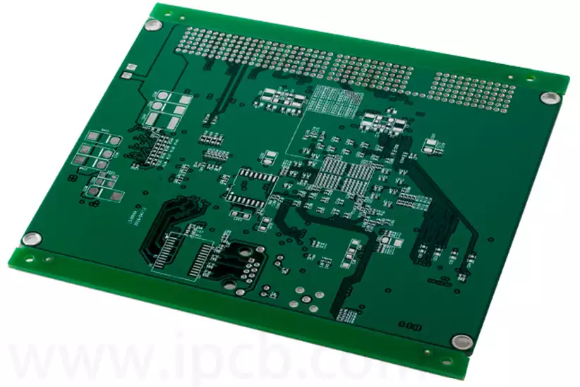
As an important basic component of electronic products, the stability of pcb substrate dimensions during the manufacturing process of printed circuit boards directly affects the performance and reliability of the final product. However, substrate dimensions often change due to a variety of factors during the production process, resulting in dimensional deviations, bending and warping, and other quality problems.
Printed circuit board manufacturing process substrate size changes
(1) The difference between the warp and weft direction caused by the pcb substrate size changes; due to shear, did not pay attention to the direction of the fibre, resulting in shear stress residual in the substrate, once the release, the direct impact of the substrate size of the contraction. Solution: determine the pattern of change in the direction of warp and weft, in accordance with the shrinkage rate on the substrate for compensation (light painting before this work). At the same time cut according to the fibre direction of processing, or according to PCB manufacturers in the substrate provided by the character mark processing (generally the vertical direction of the character for the longitudinal direction of the substrate).
(2) Copper foil on the surface of the pcb substrate partially etched away on the substrate changes in the limit, when the stress is removed to produce dimensional changes. Solution: In the design of the circuit should try to make the entire board surface distribution uniform. If it is not possible must also be in the space to leave the transition section (does not affect the position of the circuit mainly). This is due to the plate using glass cloth structure in the warp and weft yarn density differences and lead to differences in the strength of the plate in the warp and weft direction.
(3) Brush the plate due to the use of excessive pressure, resulting in pressure and tension stress resulting in deformation of the pcb substrate. Solution: should be used to test brush, so that the process parameters in the best state, and then brush the board. For thin substrates, cleaning treatment should be used chemical cleaning process or electrolysis process.
(4) The resin in the pcb substrate is not fully cured, resulting in dimensional changes. Solution: take the baking method to solve. In particular, baking before drilling, temperature 1200C, 4 hours to ensure that the resin is cured to reduce the impact of heat and cold, resulting in deformation of the size of the pcb substrate.
(5) Especially multilayer boards before lamination, poor storage conditions, so that the thin substrate or semi-cured sheet of moisture absorption, resulting in poor dimensional stability. Solution: The inner layer of the substrate treated with oxidation must be baked to remove moisture. And the treated substrate is stored in a vacuum drying oven to avoid moisture absorption again.
(6) Multi-layer pcb board by pressing, excessive flow of glue caused by glass cloth deformation. Solution: need to carry out process test pressure, adjust the process parameters and then press. At the same time can also be based on the characteristics of the semi-cured sheet, select the appropriate amount of glue flow.
Bending (BOW) and warping (TWIST) of the pcb substrate or multilayer circuit board after lamination.
(1) Especially when thin substrates are placed vertically, it is easy to cause long-term stress superposition. Solution: For thin substrates should be placed horizontally to ensure that the substrate internal stress uniformity in any direction, so that the substrate size change is very small. Must also pay attention to the original packaging form stored in a flat shelf, do not remember to stack high and heavy pressure.
(2) Hot melt or hot air levelling, the cooling rate is too fast, or improper cooling process. Solution: Place on a special cooling plate to naturally cool to room temperature.
(3) The pcb substrate in the processing process, a longer period of time in the hot and cold alternating state of processing, coupled with uneven distribution of stress within the substrate, causing the substrate bending or warping. Solution: take technological measures to ensure that the substrate in the hot and cold alternation, adjust the cold, hot transformation speed, in order to avoid sudden cold or hot.
(4) Insufficient curing of the pcb substrate, resulting in internal stress concentration, resulting in the substrate itself produce bending or warping. Solution: A: Re-curing according to the hot pressing process method. B: In order to reduce the residual stress of the substrate, improve the dimensional stability of the printed board manufacturing and warping deformation, usually using pre-baking process that is at a temperature of 120-1400C 2-4 hours (according to the board thickness, size, number of options).
(5) The differences in the structure of the substrate below the copper foil thickness. Solution: should be based on the principle of lamination, so that the two sides of the different thickness of the copper foil produced by the difference, turn to take a different thickness of the semi-cured sheet to solve.
Poor substrate with localised whitening, plates subjected to inappropriate mechanical impact or localised plates subjected to infiltration of fluorine-containing chemicals, leaching of glass fibre cloth weave points. May affect the appearance and electrical connection of signals. Need to use high Tg sheet; minimise or reduce excessive vibration of mechanical processing; choose appropriate lead desorption solution and operation process.
Substrate bad dew cloth, cause: bonding sheet resin content is low or fluidity, laminating too much flow of glue; or laminating temperature and pressure too fast, high pressure too early, resulting in too much flow of glue. Impact: cause the insulation performance of the substrate degradation, seriously affect the quality of the PCB board. Avoid: you can use the ‘table material’ and ‘material’ approach, so that the table material resin content to increase the appropriate and adjust the corresponding GT and RF% and other technical parameters, the product should be sufficient curing temperature and curing time in the hot press, you can prevent the phenomenon of dew and improve the cloth pattern. Chemical resistance and electrical properties of the pcb substrate.
Tear film is not clean and easy to seep copper, reason: not the oxidation layer of the copper foil to deal with clean, after the pressure of the film, resulting in poor bonding, or in the line to the plating process is too long, resulting in the oxidation of the copper foil within the dry film. Impact: cause short circuit, repair board thick patch line will affect the appearance. Avoidance: If it is caused by the grinding board, you need to adjust the parameters, as well as pressure dry film operating practices, as well as the tightness of the roller.
Accurate control of pcb substrate size changes and reasonable response to various types of problems in the manufacturing process is to ensure the quality of printed circuit boards and the key to performance. Through scientific process management and standardised operation, the stability and reliability of products can be effectively enhanced to meet the ever-increasing demands of the electronics industry.