In the PCB manufacturing process, pcb test points, as a key element, play an important role in ensuring that circuit testing and debugging is carried out smoothly. Their existence not only enhances the reliability of the circuit, but also effectively reduces production costs and significantly improves manufacturing efficiency.
The role of test points is broad and far-reaching. Diverse testing equipment such as multimeters, oscilloscopes, and network analyzers allow us to test all aspects of a circuit, including connectivity, resistance, capacitance, power, and frequency. This comprehensive testing greatly improves the efficiency and speed of testing, maintenance and debugging, thus shortening the product development cycle. During the manufacturing process, the test points also help us to check the quality and reliability of the PCBs, ensuring a high shipment rate and quality standards.
Test points on PCBs are mainly divided into two categories. One category is easily accessible to technicians using handheld test equipment. To address this need, we typically solder terminals to these points to clamp the test leads. These test points are marked with a reference mark, such as “GND”, for easy reference and identification.
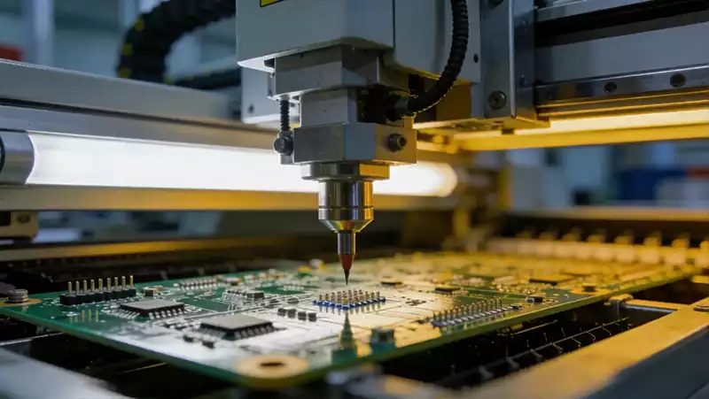
Another type of test point is designed for automated test equipment. They usually appear as through-hole pins, via holes, or small metal pads designed to accommodate the probes of an automated test system. There are three main types of test systems that utilize these PCB test points: bare board test, in-line test, and flying probe test.
Bare board testing is performed after the board has been manufactured to ensure that all networks are electrically connected. In-line testing is performed after the board is assembled, and each individual network is tested with probes in ICT fixtures. Flying probe testing is similar to ICT in that it also tests each network on the board by accessing test points after assembly. The difference, however, is that flying probe devices use probes that can be moved to each test point, rather than fixed probes like ICT.
So why are test points so important to PCB manufacturing? Automated testing is critical to verifying the manufacturing quality of printed circuit boards. Bare board testing will check that the manufactured board has good connections, while ICT and flying probe testing will verify board assembly and solder connections.
ICT and flying probe testing have a wide range of practical applications. ICT is a system that uses test fixtures and accompanying software designed specifically for a particular board. By using test point locations and other design data generated from a CAD database, we can create fixtures and software where each network will be tested using a single probe.The primary purpose of ICT is to verify board assembly by testing each network and its associated component pins for good connections, but it can also be used to test board functionality.
Although the development of ICT test equipment and software is both expensive and time-consuming, once developed, in-line testing will be able to test large numbers of boards very quickly. For mass production, the advantages of speed and functional testing quickly offset the development time and cost of ICT.
The flying probe test system is designed to verify the integrity of assembled boards, but is different from ICT. Instead of test fixtures, it uses two to six probes that can be flown to each test point on the board. Flying probe systems can be installed quickly and inexpensively, eliminating the need to build expensive test fixtures. In addition, any board changes that require changes to the test system can be easily reprogrammed. The disadvantage of flying probes, however, is that they are slower. whereas ICT can test all points on a board almost immediately, a flying probe system must move its probes to each individual test point. On large boards, this can take a long time and eliminates the ability to perform functional tests. However, for prototyping or small volume production, using flying probes as PCB test points can be very beneficial.
The rule set for test points is equally important in PCB design. The number and location of test points need to be determined according to the specific requirements of the circuit in order to avoid conflicts with the electronics that need to be installed. At the same time, we also need to pay attention to the installation of test points and board interfaces and connectors to ensure connectivity and ease of use in the actual test use.
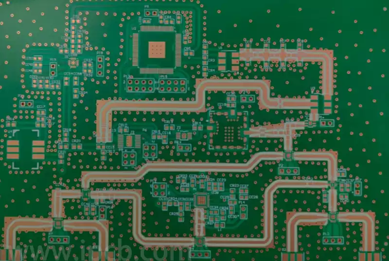
The setup of test points should be standardized and carried out in accordance with certain pcb layout rules. For example, each test point should be reasonably distributed during PCB wiring design. We can locate the test points according to the schematic diagram and arrange them centrally where they are logically or functionally identical. Reasonable test point setup helps test, debugging, maintenance, etc. to run smoothly.
In addition to the location, the shape and size of the test points should also conform to the specification. Practical test point shapes are usually small holes and marked lines for connecting two test pins for testing.
Although the test point is only a small part in the PCB, it has an important impact on the reliability, production cost and quality of the whole circuit. When setting up test points, we should arrange them according to the requirements of the circuit and strictly follow the specifications and layout rules. At the same time, during the design process, we also need to give full consideration to the location, shape and size of the test points, in order to improve the reliability and ease of use of the test, and lay a solid foundation for the manufacture of high-quality PCB.