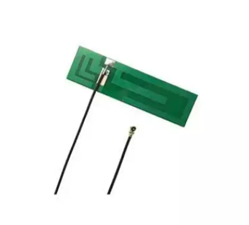
Onboard antenna refer to antennas directly integrated onto a printed circuit board (PCB). Compared to traditional external antennas, they offer advantages such as compact size, low cost, and manufacturing flexibility.
The operating principle of onboard antenna involves designing and routing conductive traces or metal lines on the PCB to enable wireless signal transmission and reception. Common forms include microstrip lines, patch antennas, and helical antennas.
For transmission, the onboard antenna receives electrical signals from an RF source. These signals are transmitted via conductors or metal traces to the antenna structure, where they are radiated as electromagnetic waves to achieve wireless signal transmission.
For reception, the antenna converts received electromagnetic waves back into electrical signals. These signals are then transmitted via conductors or metal traces to the receiver, enabling wireless signal reception.
Typical Onboard Antenna Structures
- Inverted L Antenna
Principle Overview
The inverted L antenna can be viewed as a variant of the half-wave dipole antenna. One end connects to the RF feed, while the other remains open. Due to physical space constraints, its length is typically designed as 1/4 of the operating wavelength, relying on inductive tuning for impedance matching.
Structural Features
The main arm forms an L-shape, with the horizontal segment radiating and the vertical segment coupling near the ground.
Significant capacitive effects near the ground alter the resonant frequency.
Inductors are usually connected in parallel at the feed point to compensate for distributed capacitance and tune impedance.
Design Optimization Recommendations
When spatial constraints prevent a full-length L-arm, serpentine traces or folded structures can extend the equivalent electrical length. Closer proximity to the ground plane increases parasitic capacitance, requiring simulation or debugging to optimize matching inductance.
Field strength distribution is asymmetric, making it suitable for directional or localized transmission scenarios.
- Inverted-F Antenna
Principle and Evolution
The inverted-F antenna modifies the inverted-L structure by introducing a shorting conductor to ground, forming a shape resembling a “lying-down F.” This shorting conductor acts as a parallel inductor, enabling precise tuning of the resonance point and impedance matching.
What key considerations exist for PCB design of inverted-F antennas?
Antenna length isn’t arbitrary—to minimize design, it’s typically set to 1/4 wavelength of the RF carrier. For custom designs, simulation tools are recommended.
Ground plane and feed point must be precisely matched to achieve 50Ω impedance.
The ground feed point requires a highly reliable ground connection.
The ground plane must contain a sufficient number of vias.
Clearance must be maintained around the antenna and its corresponding copper layers to prevent copper from obstructing signal radiation. This antenna exhibits significant parasitic capacitance with other copper layers.
The feed line should be short and straight.
Key Elements and Considerations for PCB Antenna Feed Line Design
Frequency:
Determine the target operating band (e.g., 2.4GHz-2.5GHz for Wi-Fi/Bluetooth, 868/915MHz for LoRa, 5GHz for Wi-Fi). The antenna’s physical dimensions (especially radiator length) are directly related to wavelength (λ). λ = c/f (where c is the speed of light and f is frequency).
PCB Material:
Substrate Material: FR4 is most commonly used (low cost), but its dielectric constant is unstable and it has a high loss tangent (especially in the GHz band), which reduces antenna efficiency and bandwidth. For high-performance requirements (e.g., 5GHz Wi-Fi, GNSS), high-frequency materials like Rogers or Taconic are typically used (low loss, stable performance).
Laminate thickness: Affects antenna impedance and bandwidth
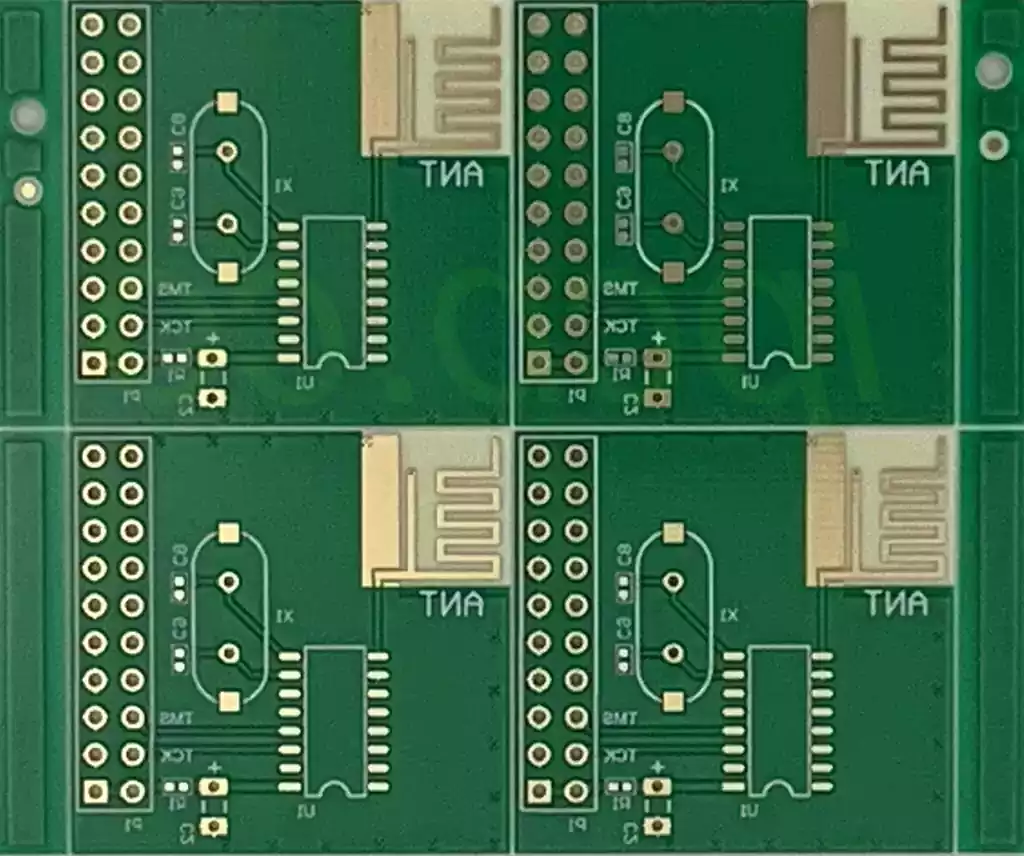
Antenna Zone (Keep-out Area/No-Cu Area):
This is the most critical physical constraint in design. For optimal radiation, all ground planes (GNDPlane) and traces must be strictly removed beneath the antenna’s key radiating structure (especially the open edge/radiating edge of IFA/PIFA across all layers) and within a specific radius around it, forming a “clearance zone.”
This area must remain free of any components, vias, or metal.
Its size and shape directly impact antenna performance and tuning difficulty. Insufficient keep-out area is a primary cause of design failure.
Ground Plane:
Antennas (especially monopole types like IFA/PIFA) require a well-defined reference ground plane to function. This plane acts as the “mirror image” of the antenna system.
The ground plane’s size, shape, and integrity (avoiding segmentation) are critical for antenna impedance matching, directivity, and efficiency. Typically, the ground plane must be at least 1/4 wavelength in size.
Antenna Feed Point and Trace Design:
Connect the antenna feed point to the RF transceiver (RFIC/module).
Impedance Control: The feedline must be designed as a microstrip line or coplanar waveguide with a 50Ω characteristic impedance. This requires strict control over trace width, PCB dielectric constant, copper thickness, and distance from the ground plane.
Length: Keep it as short as possible to minimize loss and parasitic effects. Avoid unnecessary bends.
Avoid Via Placement: Especially near the antenna radiator and feed point.
Impedance Matching Circuit:
Even with a well-designed antenna, actual impedance rarely matches 500Ω perfectly due to PCB tolerances, component pads, vias, etc.
Typically, a π-type or T-type LC impedance matching network (π-type is more common) is designed near the feed point.
This network allows precise tuning of the antenna’s resonance point and impedance (typically tuned near the center of the Smith chart) during production or debugging by replacing SMD components with different values of inductance (L) and capacitance (C).
Tuning requires a vector network analyzer.
Impact of Nearby Components and Metals:
Batteries, shielding covers, metal enclosures, connectors, and even large capacitors or inductors on the PCB can severely degrade antenna performance (causing frequency shifts and reduced efficiency).
These factors must be considered during layout, adjusting clearance zones or relocating the antenna as necessary.
Directivity and Polarization:
PCB antennas typically exhibit omnidirectional but non-uniform radiation patterns (with null points in specific directions). Designers must understand the directional requirements of the target application (e.g., watches often orient the direction of maximum radiation toward the back of the hand/outer side).
The most common polarization is linear polarization (vertical or horizontal, typically determined by the antenna structure).
Onboard antenna technology enables miniaturization and cost reduction in wireless communication by directly integrating antennas onto circuit boards. Its design core lies in comprehending and precisely controlling the relationship between antenna physical dimensions and operating frequency, while fully accounting for the impact of PCB materials on performance.