PCB prototyping is the printed circuit board in mass production before the trial production, the main application for electronic engineers in the design of the circuit, and complete the drawing of the PCB, to the circuit board factory for small batch trial production process, that is, PCB sampling.
PCB prototyping preparation
- To advance the documents, process requirements, the number of manufacturers, then there will be professionals for you to quote, order, and follow up on the production schedule.
- According to the requirements of the engineering data MI, in line with the requirements of the large sheets of sheet metal, cut into small pieces of production boards. Meet customer requirements of small pieces of plate material, the process is summarized as follows: large plate material → cut board according to the requirements of MI → curium board → beer rounded corners grinding → out of the board.
pcb circuit board proofing process
- Printing: the drawn circuit board is printed on transfer paper, pay attention to the slippery side of the face of their own, generally print two circuit boards, that is, a piece of paper to print two circuit boards. Select the best printing effect in which the production of circuit boards. With a well-drawn bottom drawing of the board photographic plate, the layout size should be consistent with the size of the PCB substrate.
- PCB photographic plate: flexible cut – exposure – development – fixing – washing – drying – plate repair, it is important to note that the implementation of the photographic should be checked before checking the correctness of the base map, before exposure, should be adjusted to the focal length of the double-sided plate should be to keep the front and back side of the photographic plate of the two focal lengths are the same.
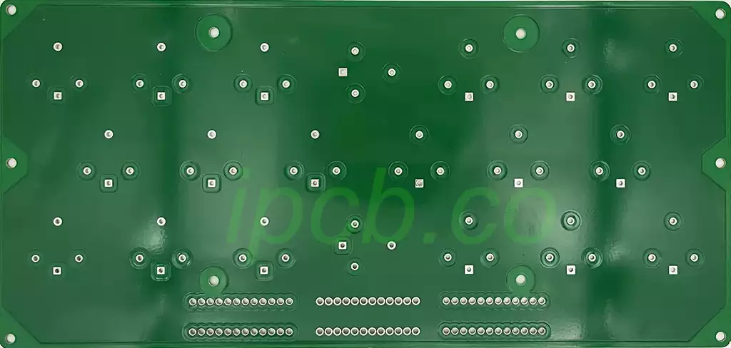
- Cutting copper-clad plate: the whole process of making circuit boards with photoconductive boards illustrated .
- Pre-treatment of copper-clad board: fine sandpaper to the surface of the copper-clad board oxide layer polished off to ensure that in the transfer of circuit boards, thermal transfer paper on the toner can be firmly printed on the copper-clad board.
- Transfer: cut the printed circuit board to the right size, paste the printed circuit board side on the copper-clad plate, align the copper-clad plate into the thermal transfer machine, make sure that there is no misalignment of the transfer paper when you put it in.
- Corrosion: PCB by the surface of the metal coating, according to different needs can be fluxed or soldermask processing.
- Drilling: according to the thickness of the electronic component pins to choose different drilling needles, in the use of drilling machine drilling, the circuite board must be pressed steadily, the speed of the drilling machine can not be too slow, drilling should pay attention to the safety of the operation.
- Pretreatment: After drilling, use fine sandpaper to sand off the toner on the circuit board, clean the circuit board with water. After the water is dry, use rosin water coated on the side of the line, and use a hot air blower to heat the pcb board, so that the rosin fast solidification.
- Test and final inspection: Welding completed on the board of electronic components, through the electronic 100% test, detection of visual not easy to find to the open circuit, short circuit and other defects affecting the functionality of the defects, and these defects are repaired to avoid problems and defects in the board out.
In PCB manufacturing, sampling is very important, mainly for the following reasons:
The merit and reliability of the sample can be used as a basis for evaluating the production process and equipment performance;
The use of sample production (proofing) process, you can test and evaluate new materials, new processes, new designs, as well as new production equipment and technology, to ensure that they can meet the expected results in the formal production;
The proofing process not only helps PCB manufacturers to improve and optimize the production process, but also improves production efficiency, reduces costs, and ultimately ensures that the product is of high quality and superior performance;
For customers, the proofing stage provides an opportunity to understand the actual quality of the final product before formal mass production, so as to make an informed decision on whether to continue cooperation;
For design engineers and customers, prototyping is an efficient and less costly mode of collaboration for verifying the feasibility and practicality of design solutions;
If problems are found during the sampling stage, they can be quickly identified and solved, thus avoiding the economic losses that may be brought about by direct mass production.
PCB prototyping as a key step in electronic product quality and efficiency assurance, in the manufacturing process of electronic products play an irreplaceable role. It is not only an important pre-production trial link, but also an important means to test the production process, equipment performance, new materials, new processes, new designs and new production equipment and technology. Through sampling, we can not only optimize the production process, improve production efficiency, reduce production costs, but also ensure the high quality and excellent performance of the final product.