PCB Resistor Calculator, also known as Chip Fixed Resistor, is a tool for calculating the resistance value of chip resistors. It can calculate the required chip resistor type and resistance value according to the user’s input parameters such as resistance value, accuracy, package type, and so on. Using Chip Resistor Calculator allows you to easily and quickly select the right chip resistor, avoiding problems such as mismatched resistors or circuit failures caused by manual calculation or improper selection.
The SMD portion of chip resistors refers to surface mount devices, which can be mounted directly onto PCB circuit boards using “surface mount technology” (SMT). The invention of surface mount technology has reduced both the size of components and the time required to manufacture circuits. SMD resistors are usually only used in professionally manufactured PCBs. For most homemade circuits, used are the more classic “through-hole” technology resistors. The reason for using through-hole resistors is that they are much easier to install and do not require specialized equipment like chip resistors.
How to Use Chip Resistor Calculator
- Input Resistance Value: Input the desired resistance value in the Chip Resistor Calculator, usually in Ohm (Ω).
- Select Precision: Select the precision level of chip resistor according to the actual need, generally there are different precision levels such as 1%, 5%, 10%, etc. to choose from.
- Select Package Type: Select the package type of chip resistor according to the actual need, generally there are 0805, 1206, 2010 and other different package types available.
- Calculation results: According to the input parameters, Chip Resistor Calculator will automatically calculate the required chip resistor type and resistance value, and give the corresponding recommended value.
Chip Resistor Calculator Notes
- Understand the basic knowledge and experience of electronic circuits: The use of chip resistor calculator requires certain basic knowledge and experience of electronic circuits, the user needs to understand the basic concepts of resistance and calculation methods, as well as the meaning of the chip resistor package type and precision level and other parameters and selection methods.
- Ensure the accuracy and reliability of the calculation: When using the chip resistor calculator, it is recommended that the user first understand the relevant basic knowledge and experience in electronic circuits to ensure the accuracy and reliability of the calculation.
- Pay attention to the usage environment of chip resistors: The usage environment of chip resistors has a certain impact on their performance, and users need to choose suitable chip resistors according to the actual situation.
What is PCB alignment width?
The alignment width is one of the most critical factors in PCB design.
Only people who often do circuit design will know that the problem of alignment width is often encountered. Some designers with little experience at the beginning prefer to use the default alignment width given in the PCB Layou software.
For experienced people, the default alignment widths have some reference value, but may be judged by some experience to be too narrow for some tracks, especially for power and ground connections.
What is an alignment?
PCB alignments are thin conductive copper wires placed on a non-conductive or isolated substrate to carry signals and power throughout the circuit. Copper alignments have a specific width, which we call alignment width, and a specific height or thickness.
Typically, the thickness of a PCB with a copper layer is fixed and determined by the specifications of the PCB manufacturing company. For a typical PCB, the most common copper thickness is 35µm, which equals 1oz/sqr ft.
So in design, we can only control the width of the alignment. For most manufacturers, the minimum alignment width is 6mil or 0.152mm, mainly due to etch process and target yield limitations.
However, in order to have a certain tolerance, an alignment of 0.254-0.3 mm is usually used.

How to calculate PCB alignment width?
- Use PCB alignment width calculator
You can use an alignment width calculator to determine the alignment width based on ampacity. However, you need to provide the design specifications in the alignment width calculator, including the maximum current (in amperes) that will flow through the alignment, the total length of the path, the temperature rise due to the resistance of the alignment, and so on.
Once the specifications are provided, the calculated width of the alignment will be automatically generated, which is usually the minimum width required. It is possible to allow current to pass safely without causing damage to the PCB.
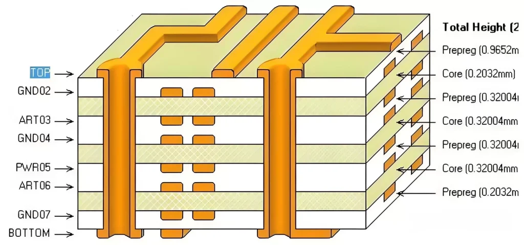
You may find that the inner layers have wider alignment widths than the outer layers because they tend to generate more heat. The outer layers will not get as much heat due to convection.
For safety reasons, it is recommended to use the entire inner PCB alignment width.
- Using the Equation
1) PCB Alignment Width Chart
PCB alignment width table can help you to determine the PCB alignment width, also can let you understand the impact of current carrying capacity and temperature rise.
2) PCB alignment width formula
According to the definition of IPC 2221, you can use the formula for calculating the allowable current through the alignment to find the PCB alignment width. The process is as follows
I=kΔT^0.44A^0.725
I represents the current and is taken as a constant
ΔT is the change in temperature
A is the cross-sectional area of the alignment.
The formula can now be rearranged to derive the trace width by finding the cross-sectional area through which the chosen currency safely passes.
Area [mils^2] = (current [amps]/(k*(temperature rise [degrees Celsius])^ 0.44))^(1/0.725)
k = 0.048
Then, consider the thickness of the alignment in order to find the desired width.
Width [mils] = Area [mils^2]/(Thickness [oz]*1.378[mils/oz])
This formula can be used for currents from 0 to 35 A and allows temperatures to rise from 10 °C to 100 °C. This formula can be used for currents from 0 to 35 A, allowing temperatures to rise from 10 °C to 100 °C. It accommodates a trace width of 400 mils, and you can use copper values from 0.5 to 3 oz.
By plugging 2 A into the above calculation, we get at least about 30 mils of trace. But you can’t calculate the voltage drop because you need to calculate the circuit of the alignment. Here’s how to calculate the alignment circuit.
How do I calculate the PCB alignment resistance?
Circuits that contain sensitive components, such as wireless chips or antennas, may need some extra protection from external noise. You can minimize the need for additional protection by embedding ground vias between the alignments, which can significantly reduce off-board signals that are coupled, picked up by nearby alignments or planes, and sneak into the board edge.
The size and shape of the copper alignment on the PCB directly affects board size, cost, and performance. In this case, the width of the PCB trace is very important. Due to higher current requirements, the traces used to carry power signals need to be wider. PCB trace width is inversely proportional to trace impedance. The following equation calculates the trace impedance:
ρ = resistivity of copper | α = temperature coefficient of copper | T = trace thickness
W = Width of trace | L = Length of trace | t = Temperature
In addition to the trace width, the shape of the trace also affects signal reflection.Asymmetrical trace dimensions and sharp bends can cause signal reflections that can lead to signal distortion. In multi-layer PCBs, power signal alignments are usually placed on the top layer to improve heat dissipation. On the other hand, data signal alignments are placed on internal layers to protect against EMI and environmental noise.
PCB Resistor Calculator and PCB Alignment Width Calculation are integral parts of electronic design, and their accuracy and reasonableness directly affect the performance and reliability of the circuit. For electronic engineers, mastering these techniques and tools is the key to improving design quality and efficiency.


