Screen printing is the process of producing printed circuit boards using silkscreen printing technology. The screen printing layer is one of the layers used to label components or add other information when drawing PCBs. Through this printing method, the component shape, serial number and other descriptive text printed on the component surface or solder surface to facilitate the production process of the circuit board plug-in, including the surface of the encapsulated components of the patch, as well as the future product maintenance operations.
PCB silkscreen contains what information
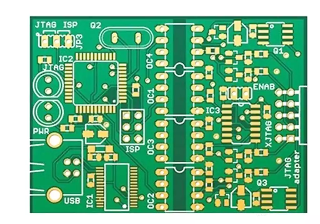
- Polarity reference mark
- Determine the test point A
- Component bit number reference mark
- Component boundaries
- Component pin marking
- Unique identification number for each board
- Company logo
- Version number
- Date code
- Manufacturer’s logo, serial number, lot number
- Warning symbol
- Regulatory markings
Regulatory markings are used to indicate that a design has been inspected or complies with specific regulations.
RoHS, FCC, CE, and e-waste symbols are usually found on consumer and commercial products that have passed the relevant inspections.
If you see another mark on a safety-checked design: the UL Mark, this indicates that the design was manufactured and assembled by a UL-certified manufacturer in accordance with UL796 and UL94 standards.
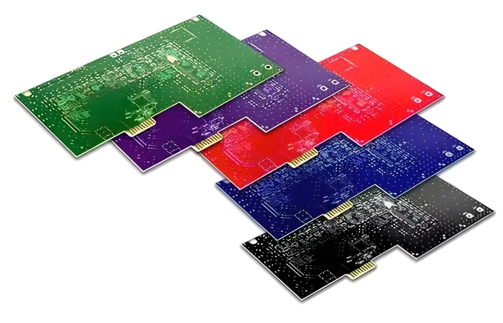
What colors are available for PCB silkscreen?
Typically, PCB silkscreen colors are white, which is a public color and is manufacturing friendly.
In addition, other colors such as yellow, red, and black are commonly used in the initial stages of PCB board design. Pink silkscreen is a favorite color for some PCB Layouts (not me anyway), but it is usually not recommended because it has specific characteristics that are not friendly to the manufacturing process.
Silkscreen Design Requirements
Silk-screened characters of the word height and word width ratio, the general requirements ≥ 6:1, there are three common font size: Among them, the board density is relatively large, commonly used 4/25mil characters (No. 1); conventional density, the recommended 5/30mil characters (No. 2); board is more loose, the recommended 6/45mil characters (No. 3); usually the surface layer of the base layer of the thickness of the copper screen print the width of the corresponding requirements, the base of the copper < 1OZ, limit value ≥ 4mil, optimized value ≥ 6mil; base copper thickness of 1OZ, priority use 5/30mil characters; base copper 2OZ, priority use 6/45mil characters.
Add PCB screen printing requirements
- Placement: In general, resistors, capacitors, tubes and other devices screen printing, placement, do not use the four directions, which will lead to debugging, maintenance, welding, looking at the screen printing to see a very tired (board to turn a few directions).
- Try not to hit the silkscreen over the hole.
- Silk screen do not press on the high-speed signal lines (such as, clock lines, etc.): for the top or bottom of the high-speed signal lines, because these signal lines, can be regarded as microstrip lines.
- silkscreen reading direction to be consistent with the direction of use of silkscreen reading direction and the use of the chip in the same direction, mainly when welding, to reduce the probability of welding reverse.
- The silkscreen should be clearly labeled pin number.
- Special package silkscreen: for BGA, QFN and other special packages, the size of the silkscreen with the chip size is identical.
- Mounting holes silkscreen: mounting holes near the screws to increase the silkscreen, while indicating the length and the total number of screws, to facilitate the installation.
Design considerations
- Screen printing line width on the board ≥ 4mil, to avoid electronic components screen printing line width of 0.
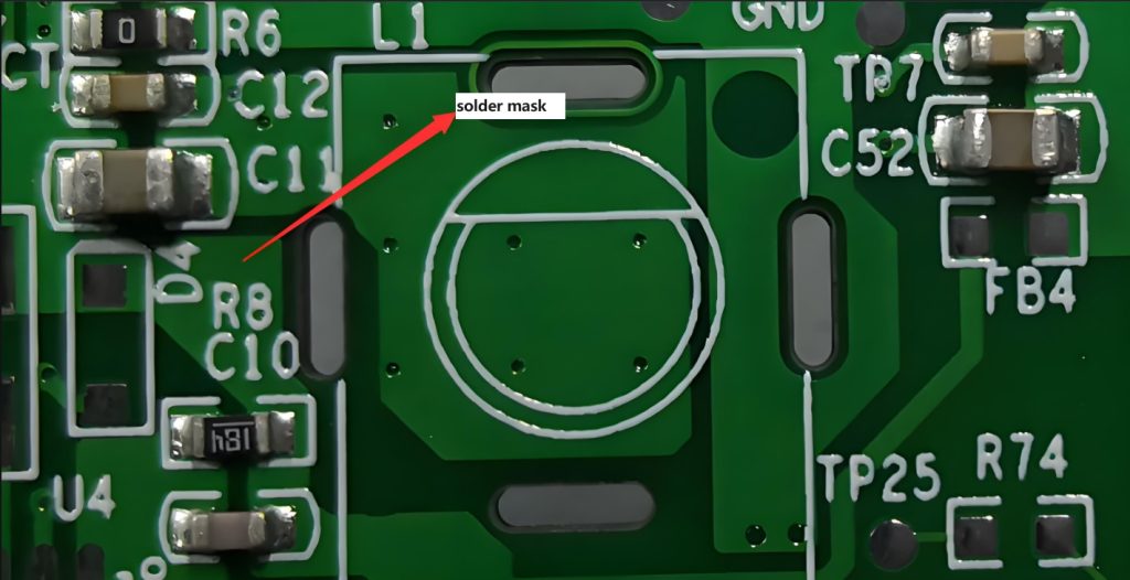
- silkscreen and pad spacing: silkscreen do not cover the weld points on the board, such as SMD device pads, plug-in through-hole, silkscreen as an insulating material, once on the pad, will lead to poor welding; also do not cover the board test points, mark points, etc.; usually required to maintain a 6mil spacing.
- Spacing between the screen prints: keep 6mil, screen prints between the overlap is acceptable, once the overlap leads to unrecognizable, it is necessary to adjust away.
- Screen Printing Direction: The screen printing string arrangement should follow the principle of left-to-right or bottom-to-top when the string is viewed from the front.
- Device bit number placement: device bit number should be one-to-one correspondence with the device, can not be reversed, change the order; when the density of devices is relatively high, you can use the lead out of the labeling or symbols labeling method,will be placed on the board in other places where there is room for the bit number.
- Component polarity marking and “1” foot marking to be placed correctly and clearly.
- Lead out of the labeling or symbol labeling, the added silkscreen, characters should be placed on the Board Geometry silkscreen layer.
The added board name and version number silkscreen should also be placed on the silkscreen layer of Board Geometry. - The device bit number cannot be placed inside the device or outside the board frame.
- When the density of the board is relatively high, there is really no space to place the bit number, you can discuss with the customer does not want the bit number, but you need to come up with assembly drawings to facilitate the guidance of device installation and inspection.
- When customers request to write copper characters in the top and bottom layers, line copper character line width: HOZ-based copper – character width of more than 8mil, height of more than 45mil; 1OZ-based copper – character width of more than 10mil, height of more than 50mil. At the same time need to do a good job of solder resist open window, so that the production of the board on the copper character is brighter.
Significance
- Identify the location and direction of components
Can identify the location and direction of the components on the board to facilitate assembly and maintenance. - Judge circuit board models and specifications
Can print circuit board model, specification and version and other information, easy to identify and manage. - Improve the quality of product appearance
You can print LOGO, production date and other information to beautify the appearance of the circuit board, improve product quality and grade, enhance corporate image and visibility. - Determine the location of the pad
Can determine the location and direction of the pads to ensure that the pads are arranged correctly. - Prevent short circuit
Components can be installed after the completion of the circuit board to draw a circle around the periphery of the prohibited welding area to avoid short-circuit accidents. - Convenient maintenance
Can identify the location and direction of the components on the circuit board to facilitate maintenance personnel to find and replace components.
Circuit board screen printing as a key process in PCB manufacturing, not only identifies the location of components and information, but also improve product quality and maintenance convenience, is to ensure that the circuit board function is perfect and efficient operation of an important part.