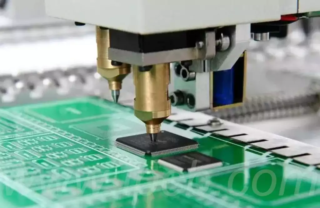
Since the copper layer on the PCB board is easily oxidized, the resulting copper oxide layer can seriously degrade the soldering quality and thus the reliability and effectiveness of the final product. In order to avoid this situation, the need for pcb surface treatment. Some information will be talking about the surface molding, board factory process will make a distinction, are considered to be the outermost layer of the PCB board and on top of the copper, to play the role of copper “coating”.
Surface treatment process
From the beginning will use flux in the copper surface soldering components, products need to be large quantities, will use electroplating tin-lead. When PCB boards are coated with solder resist, hot air solder leveling (HASL) begins to appear. Organic Solderability Protection (OSP) appears as product wiring density increases. The need for clean assembly operations, ENIG process is widely used, and then later the emergence of environmental requirements of lead-free, began to appear chemical precipitation of silver, chemical precipitation of tin, chemical nickel-palladium gold, chemical nickel-silver (ENIAg), etc.
The following is an analysis of the advantages and disadvantages of the three different surface treatment processes of HASL, ENIG and OSP:
HASL (surface tinning process)
HASL includes both leaded and lead-free tin spraying. Although this process was the dominant surface treatment in the 1980s, fewer and fewer boards are now using HASL due to the trend towards miniaturization of boards. This is because the HASL process may cause fine parts to be soldered to the tin beads, forming spherical tin spots that affect production quality. Therefore, many PCBA processors prefer ENIG and OSP surface treatment processes in pursuit of higher process standards.
The advantages of leaded spray tin is relatively low price, excellent soldering performance, and mechanical strength and gloss is better than lead-free spray tin. However, its disadvantages are also obvious, containing heavy metal lead, does not meet the environmental requirements, can not pass the ROHS and other environmental assessment.
The advantages of lead-free spray tin is affordable, good soldering performance, and relatively environmentally friendly, can pass ROHS and other environmental assessments. However, its mechanical strength and gloss are slightly inferior to leaded spray tin.
The common disadvantage of HASL is that its surface flatness is poor, not suitable for soldering pins with small gaps and too small components. During PCBA processing, it is prone to produce tin beads, which may cause short-circuits to components with small gaps in the pins.
ENIG (Immersion Gold Process)
ENIG is an advanced surface treatment process mainly used for circuit boards that require connectivity features and have a long surface storage period.
The advantages of ENIG are its high oxidation resistance for long term storage, flat surface, and suitability for soldering small gap pins and small solder joint components. Its reflow soldering can be repeated many times without degrading solderability, and it can also be used as a substrate for COB lead bonding.
However, the drawbacks of ENIG are also obvious, with its higher cost and poorer solder strength. Due to the chemical nickel plating process, it is prone to black disk problems. The nickel layer oxidizes over time and long-term reliability is problematic.
OSP (Oxidation Protective Process)
OSP is an organic film formed on the surface of bare copper, which has antioxidant, thermal shock and moisture resistance efficacy, and protects the copper surface from rusting in a normal environment. It is equivalent to an antioxidant treatment, but in the subsequent high soldering temperatures, the protective film must be easily removed by the flux, exposing the clean copper surface to combine with the molten solder to form a strong solder joint. Currently, there is a significant increase in the percentage of boards using the OSP surface treatment process for both low-tech and high-tech PCB boards. The OSP process would be the ideal surface preparation process if there are no surface connection functionality requirements or storage period constraints.
The advantage of OSP is that it retains all the benefits of bare copper soldering and expired (three months) boards can be resurfaced, but usually only once.
However, the disadvantage of OSP is that it is susceptible to acid and humidity. When used in secondary reflow soldering, it needs to be done within a certain period of time, and usually the results of secondary reflow soldering will be relatively poor. If stored for more than three months, it must be re-laid. It must be used within 24 hours of opening the package. Since the OSP is an insulating layer, the test points must be printed with solder paste to remove the original OSP layer before the pins can be touched for electrical testing, which may result in the need for major changes to the PCB assembly process. ICT will be adversely affected if untreated copper surfaces are detected. Over-pointed ICT probes can damage PCBs, requiring manual precautions to limit ICT testing and reduce test repeatability.
Each surface treatment process has its own unique characteristics and applications are not quite the same. Depending on the application of different boards for different surface treatment requirements, the choice of which surface PCB treatment process should be based on the actual use of printed circuit boards to decide.