PCB thickness usually refers to the thickness of the substrate, i.e. the distance between the conductive and insulating layers. This distance is small but has a significant impact on the overall performance of the board. The right thickness ensures the strength and stability of the board as it undergoes its daily work, while also helping to dissipate heat and control electromagnetic interference.
Printed circuit board size from the production point of view, the minimum single board should not be less than 250 × 200mm, the general ideal size of (250 ~ 350mm) × (200 × 250mm), for the long side is less than 125mm or the wide side of the PCB is less than 100mm, easy to use collocation.
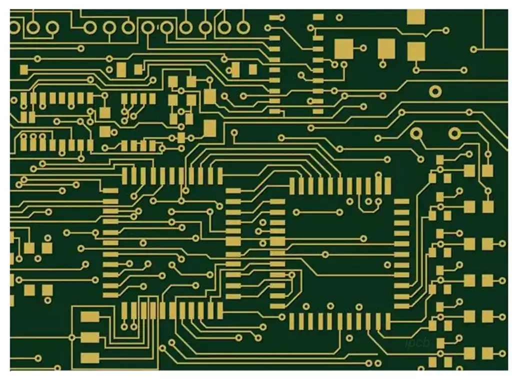
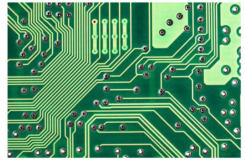
Surface assembly technology for the thickness of 1.6mm substrate bending amount of provisions for the upper warp ≤ 0.5mm,the lower warp ≤ 1.2mm. usually allowed bending rate of 0.065% or less,according to the metal material is divided into three kinds of typical PCB shown;according to the structure of the hard and soft is divided into three kinds of electronic plug-ins are also to the number of high-footed,miniaturization,SMD and complex development. Electronic plug-ins are installed on the circuit board through the pins and the pins are soldered on the other side,this technology is called THT (ThroughHoleTechnology) plug-in technology. This is done by drilling holes for each pin on the PCB board,which illustrates how circuit boards are typically used.
How to determine the PCB thickness?
Choosing the right copper pcb thickness plays an integral role in pcb assembly.There are two things to keep in mind when considering PCB copper thickness. The first factor to consider is the current thermal rise capability of the barrel.The second is mechanical strength,which is determined by the thickness of the copper,as well as the size of the plated-through-hole (PTH) and the presence of support holes.
There are a number of materials that circuit board assembly services can choose from when designing a PCB.These choices include standard FR4, which operates at temperatures of 130 degrees Celsius.High temperature polyimide is another option this material can withstand temperatures up to 250 degrees Celsius.
Tests have been conducted specifically for circuit board assembly services to determine the thermal toughness of printed circuit board assemblies. Thermal strains come from different PCB assemblies and repair processes. During these times, the difference between the coefficient of thermal expansion (CTE) and the PCB laminate drives enough power for crack nucleation as well as the extension of the circuit to failure.PCB manufacturers use thermal cycling testing (TCT) to check for an increase in the resistance of a circuit during thermal cycling at approximately 25-260 degrees Celsius. Increased resistance is a sign of reduced electrical integrity. This is usually due to cracks in the copper circuitry.
Thermal cycling test results indicate that the manufacturer’s failure rate can become unacceptable, regardless of the board material. A study of standard boards (FR4 plated with 0.8-1.2 mil copper) showed that after 8 cycles, 32% of the boards failed. Boards made from more exotic materials can have impressive improvements in this failure rate – boards made from cyanate have only a 3% failure rate.
PCB copper foil thickness setting rules
1) Standard thickness range: Common copper foil thicknesses include 1 oz (~35 μm), 2 oz (~70 μm), etc. Special applications can be customized with thicker or thinner copper foils. The selection of copper foil thickness should be based on the current density of the circuit, signal integrity requirements and cost budget.
2) Design Specification: During the design phase, engineers need to calculate the minimum copper foil area or width based on the current requirements of the circuit, and then extrapolate the required copper foil thickness. For High Density Interconnect (HDI) boards or high frequency circuits, thinner copper foils may be required to minimize parasitic effects.
3) Manufacturing constraints: The process capability of different PCB manufacturers varies,and some complex multilayer boards or special requirements may be limited by the manufacturer’s copper foil thickness. Design should be communicated with the manufacturer to confirm in advance.
4) Environmental factors: For PCBs in extreme operating environments (such as high temperature, high humidity or high vibration environment), it may be necessary to adjust the thickness of copper foil to enhance the stability and durability of the circuit.
Selection of the appropriate PCB thickness should take into account the following factors:
Application requirements: There may be differences in the mechanical strength, heat dissipation requirements, and weight limitations of PCBs for different types of electronic devices. For example, portable devices tend to choose PCB thickness to reduce weight, while industrial equipment may require thicker PCB to ensure durability and good thermal performance.
Component Layout and Package Type: High-density, mass-integrated circuit designs, or the use of large, heavy-duty components, may require thicker PCBs to provide adequate mechanical support and heat dissipation.
Cost and Manufacturing Difficulty: In general, the thinner the PCB, the more difficult it is to manufacture and the cost may increase accordingly. Conversely, thicker PCBs may lead to increased raw material consumption, which in turn drives up costs. Therefore, under the premise of meeting performance requirements, the relationship between cost and thickness needs to be weighed.
Although the pcb thickness is only a small parameter, but it has a non-negligible impact on the performance of electronic products. Through a reasonable choice and optimize the thickness of the circuit board, not only can improve product performance and stability, but also to reduce costs and improve production efficiency.