PCBA (Printed Circuit Board Assembly) integrated circuit lead forming process is an important technology in modern electronics manufacturing, which involves adapting the pins of integrated circuits to the specific shape and requirements of the board. This process plays a key role in ensuring pin soldering and product performance, which not only affects production efficiency, but is also directly related to the quality and reliability of the final product.
The main goal of lead forming is twofold: firstly, to ensure that the device leads can be accurately soldered to the corresponding pad positions on the PCBA (Printed Circuit Board Assembly); secondly, to effectively solve the problem of stress relief. When the PCBA components are completed and debugging qualified welding, will be carried out, including vibration, high and low temperature shock, including environmental stress test. These tests will pose a certain challenge to the device itself and the strength of the PCBA solder joints. The stresses generated during environmental stress testing can be partially relieved by forming the leads of the IC. This stress relief occurs primarily on all leads or wires between the lead root of the formed component and the solder joint, thus ensuring a certain degree of freedom of expansion and contraction of the leads or wires between these two critical connection points. Doing so prevents harmful stresses on components and solder joints due to mechanical vibration or temperature changes, and plays a vital role in enhancing product reliability. As a result, the forming of IC leads is receiving increasing attention in the product manufacturing sector.
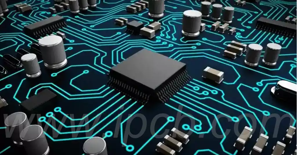
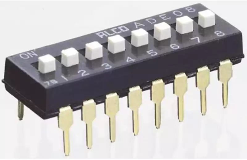
A Pin Adapter Converter is a component in an electronic device that connects different types of pins to match different circuit board design requirements. In the PCBA (i.e. Printed Circuit Board Assembly) manufacturing process, the production process of Pin Adapter Converter usually covers the following aspects:
Design: Engineers first based on the circuit design specifications, planning the specifications and form of the pin adapter, which covers the number of pins, spacing, length and other core parameters.
Material Selection:Selection of appropriate materials to manufacture the pin adapter, common materials include copper, iron, stainless steel, etc., the specific selection is based on the working environment and performance standards of the pin adapter.
Mould manufacturing:according to the design drawings, manufacturing the corresponding mould, the accuracy of the mould has a direct impact on the quality and consistency of the pin adapter.
Stamping and forming:using stamping machinery, the material is stamped into the initial form of the pin adapter, this step requires precise control of the strength and speed of the stamping, in order to ensure that the form and dimensions of the pin are up to standard.
Electroplating: In order to enhance the conductivity and corrosion resistance of the pins,it is usually necessary to implement electroplating on the pins, common plating materials such as gold, tin, nickel and so on.
Injection moulding:If the pin adapter needs to be equipped with a plastic shell, an injection moulding machine is used to inject the plastic material into the mould to form the shell component of the pin adapter.
Assembly:The plated pins are assembled into the injection moulded plastic shell to ensure a solid connection between the pins and the shell.
Quality Inspection:Implement quality inspection on the finished pin adapter,covering dimensional measurement, conductivity test,voltage resistance test,etc., to ensure that the product meets the design requirements.
Packaging: Products that pass the quality inspection will be packaged for shipment or storage.
Subsequent processing: depending on the specific needs of the customer, subsequent processing such as customised labelling,special coatings, etc. may also be required.
Throughout the production process, quality control is of paramount importance, and each step needs to follow strict operational specifications and testing standards to guarantee the performance and reliability of the final product. In addition, with the innovation of technology, automation and intelligent equipment have been gradually introduced into the production process, aiming to improve production efficiency and reduce costs.
PCBA component lead forming is for small devices, large devices can not be suspended across the joints, single independent put, must be fixed in the installation position with brackets, cards and so on. The following ipcb will introduce the method of its forming process:
- Connecting line forming process
In the connection line before the welding operation, you need to use the installation of pressure plate will short circuit line firmly pressed, and then use the clamp to install the pressure plate and the printed circuit board tightly clamped, and then the printed circuit board will be flipped (to ensure that the welding surface facing upwards) for placement. After this, the connecting wires can be soldered. The soldered wires should be carefully checked for soldering quality and any wires that are longer than required should be cut to avoid short-circuiting between the pins. - Double-pin component forming welding
Dual-pin components can be soldered by means of straddling, vertical, horizontal, etc., and need to ensure that the position of the component does not move when subjected to vibration.The bending of the lead wires is customised according to the actual distance between the solder joints. Double-pin components mainly cover resistors, capacitors, inductors, diodes, etc., in the formation of vertical or horizontal layout, and lead bending from the root of the pin to maintain a distance of at least 2mm, the bending radius is not less than twice the diameter of the lead, in order to reduce the mechanical stress, to prevent excessive bending of the lead wire due to breakage or be pulled out. - Three pins and more multi-pin components forming
This type of component pin forming needs to be strictly based on the soldering requirements to perform.Typically,these components are diodes, SCRs or integrated circuits, the common characteristic is easy to be damaged by heat,so you need to keep a longer pin for welding.For low power components, a variety of mounting methods can be used,such as positive,inverted,horizontal or horizontal mounting.
The PCBA (Printed Circuit Board Assembly) IC pin forming process and component lead forming technology are core elements of modern electronics manufacturing, and they ensure accurate and stable circuit connections and enhance product reliability.As technology iterates, these processes will continue to be optimised, providing a guarantee of high performance and quality for electronic products.
