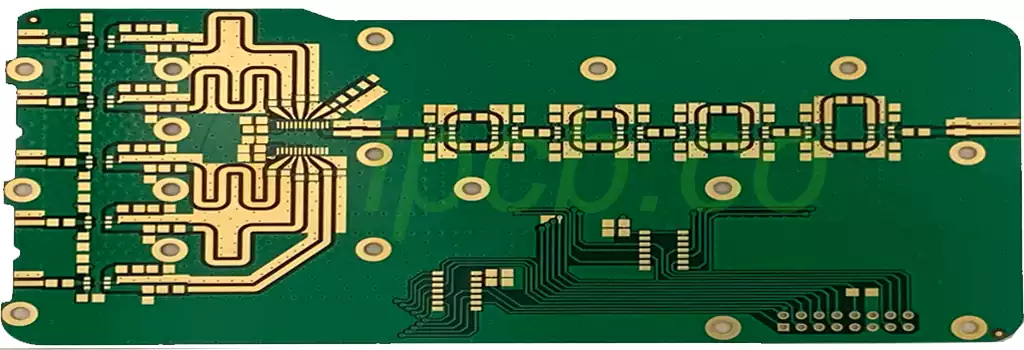
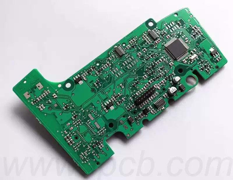
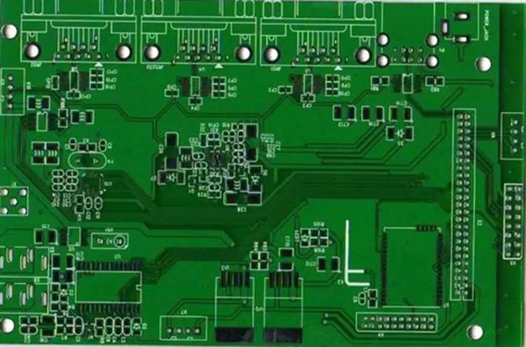
RF circuit board design is an important branch in the field of electrical engineering, which focuses on the design, optimization, and implementation of circuits and systems used to process Radio Frequency (RF) signals. RF signals usually refer to electromagnetic signals with frequencies between several thousand hertz and several hundred gigahertz, and are widely used in wireless communications, radar, satellite communications, television broadcasting and other fields.
RF circuit design is based on electromagnetic field theory and circuit theory. Designers need to master the propagation characteristics of electromagnetic waves, the theory of transmission lines, the design of matching networks, and the working principles of basic circuit modules such as amplification, filtering, modulation, and demodulation. RF circuit design usually involves the following key aspects:
Frequency selection: select the appropriate operating frequency according to the application requirements. Different frequencies have different propagation characteristics, which have an impact on antenna design, signal propagation distance, penetration capability, etc.
Impedance matching: In RF circuits, impedance matching is the key to maximizing signal power transmission. Designers need to ensure a good match between source impedance and load impedance to minimize signal reflection and energy loss.
Noise and interference suppression: RF signals are susceptible to noise and interference during transmission. Designers need to use appropriate filtering, shielding and grounding techniques to reduce noise and interference levels and improve signal quality.
Linearity and Stability: RF circuits need to maintain good linearity and stability when processing signals. Linearity determines the accuracy of signal processing, while stability is related to the reliability of the circuit for long-term operation.
RF circuit power supply design considerations
(1) The power line is an important way for EMI to enter and exit the circuit. Through the power line, outside interference can be transmitted to the internal circuit, affecting the RF circuit indicators. In order to reduce electromagnetic radiation and coupling, the primary side of the DC-DC module is required to minimize the primary side, secondary side, load side loop area. Power supply circuits, no matter how complex the form, have high current loops that are as small as possible. The power and ground lines should always be placed very close together.
(2) If a switching power supply is used in the circuit, the layout of the peripheral devices of the switching power supply should conform to the principle of the shortest return path for each power. Filter capacitors should be placed close to the relevant pins of the switching power supply. Use common mode inductors close to the switching power supply module.
(3) Long power lines on the single pcb board should not approach or pass near both the output and input of the cascade amplifier (gain greater than 45dB). Avoid power lines that become RF signal transmission paths, which may cause self-excitation or reduce sector isolation. High-frequency filtering capacitors need to be added to both ends of long power lines, and even to the center.
(4) RF PCB power inlet combination of parallel three filter capacitors, the use of these three capacitors of their respective advantages were filtered out of the power line on the low, medium and high frequency. For example: 10uf, 0.1uf, 100pf, and in accordance with the order from large to small near the power input pin.
(5) with the same set of power supply to the small signal cascade amplifier feed, should start from the last stage, in turn, the power supply to the front stage, so that the EMI generated by the end of the circuit to the front stage of the lesser impact. And each level of power filtering at least two capacitors: 0.1uf, 100pf. When the signal frequency is higher than 1GHz, to increase the 10pf filter capacitance.
(6) Commonly used in low-power electronic filters, filter capacitance to be close to the triode pin, high-frequency filter capacitance closer to the pin. Triode selection of lower cut-off frequency. If the triode in the electronic filter is a high-frequency tube, working in the amplification area, the layout of the peripheral devices and unreasonable, in the power supply output is easy to generate high-frequency oscillation. Linear voltage regulator module may also have the same problem, the reason is that there is a feedback loop within the chip, and the internal transistor works in the amplification area. In the layout of the requirements of high-frequency filter capacitors near the pin, reduce the distribution of inductance, destroying the oscillation conditions.
(7) The copper foil size of the POWER part of the PCB conforms to the maximum current it can flow, and the margin is considered (general reference is 1A/mm line width).

(8) The input and output of the power supply line should not be crossed.
(9) Pay attention to power decoupling and filtering to prevent different units from interfering through the power line, and the power lines should be isolated from each other when power wiring. Power lines are isolated from other strong interference lines (such as CLK) by ground lines.
(10) The power supply wiring of small signal amplifier needs to be isolated by ground copper skin and grounding hole to avoid other EMI interference from running in, which will deteriorate the signal quality of this stage.
(11) Different power supply layers should avoid overlapping in space. Mainly to reduce the interference between different power supplies, especially some of the voltage difference between the power supply, the power plane overlap problem must try to avoid, it is difficult to avoid can be considered in the middle of the ground layer.
(12) Printed circuit board layer distribution to facilitate the simplification of subsequent wiring processing, for a four-layer PCB board (commonly used in WLAN circuit boards), in most applications with the top layer of the board to place components and RF leads, the second layer as the system ground, the power supply part is placed in the third layer, any signal lines can be distributed in the fourth layer.
Applications of RF Circuit Board Design
RF circuit design has a wide range of applications in several fields. Here are some typical application scenarios:
Wireless communication: RF circuits are the core components of wireless communication systems, including transceivers and antennas in cellular phones, wireless local area networks (WLAN), Bluetooth, and other devices.
Radar system: RF circuits in radar systems are used to generate, transmit and receive RF signals for target detection, tracking and positioning.
Satellite communication: RF circuits in satellite communication systems are responsible for signal transmission and processing between ground stations and satellites to achieve worldwide communication coverage.
Television broadcasting: RF circuits in television broadcasting systems are used to transmit and receive television signals to ensure that viewers can receive high-quality television programs.
With its superb technology and wide range of applications, RF circuit board design shines in the fields of wireless communications, radar, satellite communications and so on. With the continuous evolution of communication technology, RF circuit design will continue to lead the development of the electronic engineering field, driving the human society towards a more intelligent and interconnected direction.


