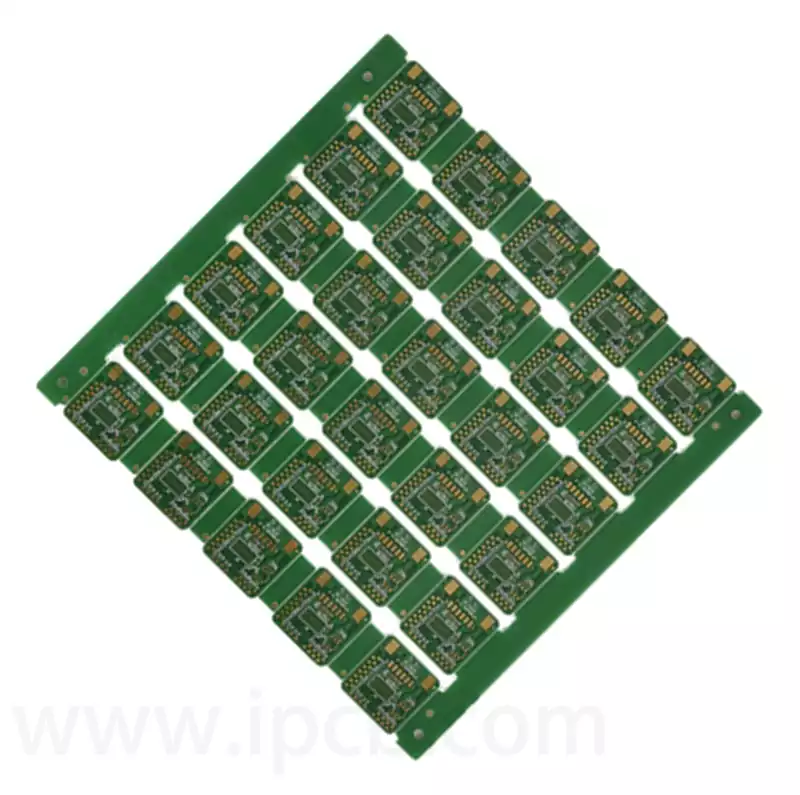
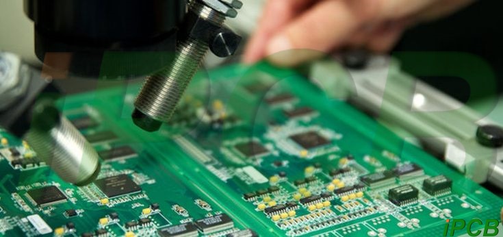
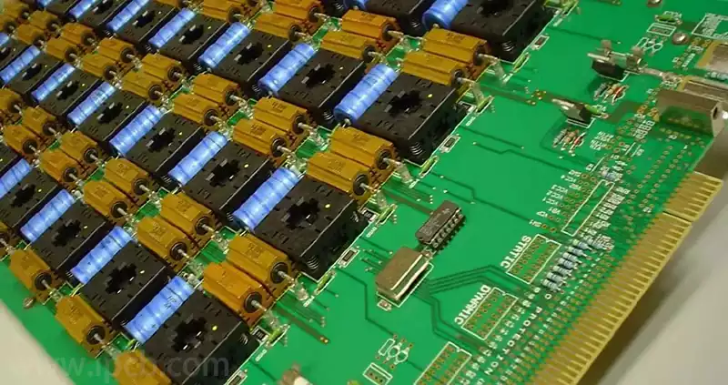
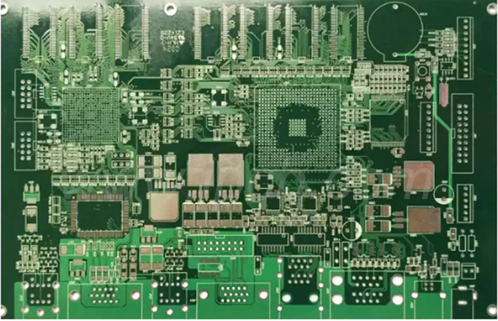
Printed circuit board drilling is a process of creating cavities, slots, or holes in a circuit board, which is usually performed prior to mounting components. Drilling can be accomplished through mechanical drilling or laser drilling, among other means, with the goal of creating the desired electrical connections and mounting locations for the circuit board. After drilling, plating is often required to ensure that the holes are electrically conductive, which in turn safeguards the circuit connections.
Holes in printed circuit boards can generally be categorized as:
Through-hole (VIA)
A through-hole is a common hole used for electrical connections between different layers of a circuit board. Its main function is to conduct circuits and allow signals to pass between different layers. A through-hole is typically used to connect the pins of electronic components, providing the necessary electrical interconnections. Moreover, it is designed so that components can be soldered directly on the surface or inside the circuit board.
Blind Vias
Blind vias are holes that are located between the top and bottom layers of a printed circuit board and are used to connect the inner layer of wiring without penetrating to the other side of the board. This type of hole saves space and increases the density of wiring between layers. Blind vias are generally no deeper than a certain percentage to ensure that the plating process runs smoothly, as well as to avoid other problems that occur when drilling.
Buried Holes
Buried holes, on the other hand, are connection holes between internal circuit layers that do not extend to the outer layers of the board. Their purpose is to increase the density and complexity of the circuitry without affecting the external structure. Similar to blind vias, the creation of buried vias requires specific production steps to ensure their functionality and reliability.
Non-Plated Holes (NPTH)
Non-plated holes are holes that are not plated and therefore do not have a conductive function. These holes are mainly used for mechanical structural needs, such as mounting fasteners or fixing devices, and help to improve the structural stability of the PCB. Non-plated holes are often referred to as mounting holes at the time of design for those application scenarios where conductivity is not required.
Thermal Through Hole
Heat through holes are a special type of via that is used to dissipate heat.Thermal vias that do not conduct current are primarily responsible for preventing high power components from generating excessive heat during operation.These holes are usually designed and used in relation to high power components on the board surface to ensure effective thermal management.
Printed Circuit Board Drilling Process
Determine the design and prepare
Before drilling can begin,the PCB design and hole layout must be defined.This step involves utilizing computer-aided design (CAD) software to generate a board layout drawing, as well as defining the size, location, and type of holes,such as through holes, blind holes, or buried holes. This is the basis for ensuring that all connections and mounting points meet the design requirements.
Pre-processing
Before drilling, the circuit board material usually needs to be pre-treated.First,it may be necessary to cover the copper layer. The completion of the pre-coating ensures that further work goes smoothly, after which the board is loaded onto a drill press ready for drilling. This process must be carried out with care to minimize the subsequent generation of burrs.
Drilling operation
The drilling operation is carried out using an automated drilling machine (usually a CNC machine) according to the design drawings. Depending on the type of hole and its size, either mechanical drilling or laser drilling technology is selected. Mechanical drilling is suitable for most holes, but laser drilling can accurately create holes with smaller diameters.
Deburring and Cleaning
Once the drilling is complete, the PCB needs to be deburred and cleaned. This step removes copper burrs created during the drilling process and cleans the walls of the holes to ensure smooth plating and surface performance. After decontamination, plating is usually performed to enhance the conductivity of the holes.
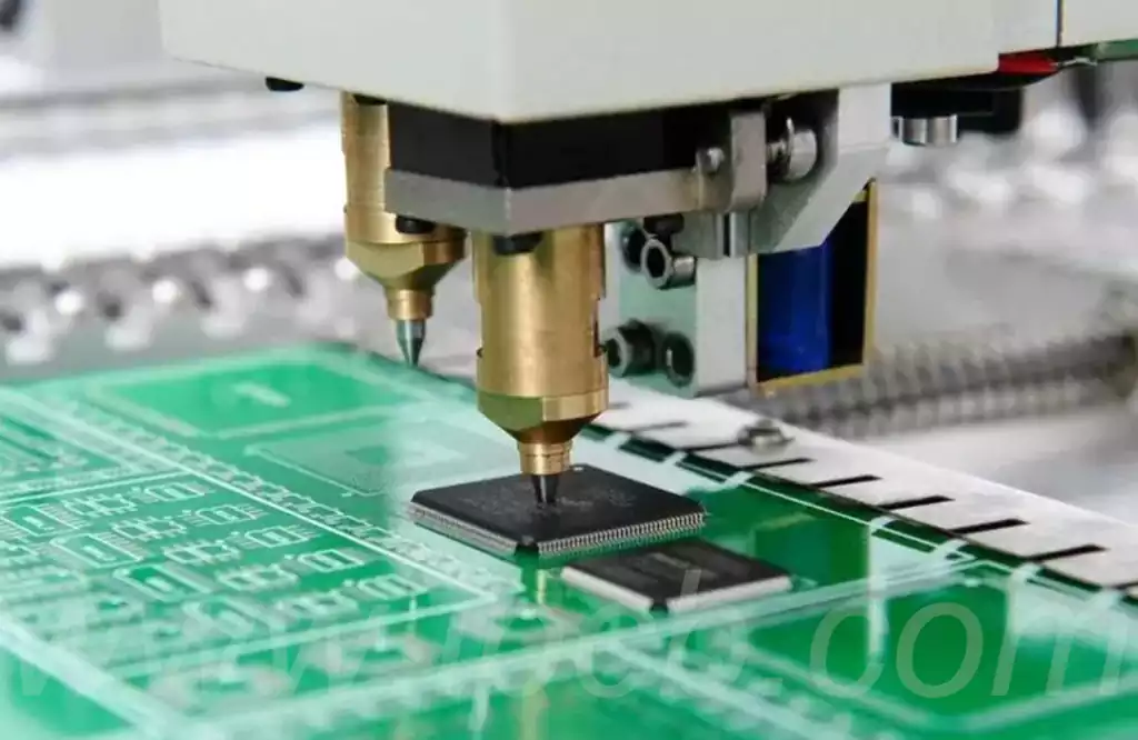
Role of Printed Circuit Board Drilling
Electrical Interconnection
One of the main roles of PCB drilling is to realize electrical connections between different layers of the board.By drilling the holes, the signals between the layers are interconnected, allowing the electronic components to function properly.
Component Mounting
Drilled holes also undertake the task of fixing and installing electronic components, so as to facilitate the accurate positioning and stable installation of components. Proper drilling ensures the performance of the components and the overall reliability of the board.
Optimizing Thermal Performance
In addition, drilling holes improves the thermal performance of the PCB. By drilling holes in designated locations, heat can be effectively directed to help maintain the board within a safe operating temperature range.
Improved Structural Stability
Appropriate hole design not only facilitates electrical connections, but also enhances the mechanical strength and stability of the PCB, reducing the risk of failure due to external interference.
Problems and solutions often encountered in the drilling process
- Hole size is not allowed
Inaccurate hole size is the most common problem, usually due to the wrong specification of the drill nozzle,drill wear or improper feed speed. In order to solve this problem, it is necessary to:
Carry out rigorous drilling quality checks to ensure that the drill bit specification meets the requirements.
Regularly check the wear of the drill bit and adjust the feed speed and rotational speed appropriately according to the material characteristics. - Leakage drilling
Leakage drilling is due to operator error or improper machine settings, resulting in part of the hole not being drilled through. Solving this problem can be done by:
Strengthening the training of operators to improve their professional skills and attentiveness.
Ensuring that machine settings are standardized and regularly maintained to avoid equipment failure. - Deviated holes
The deviated hole problem occurs when the position of the hole deviates from the intended design. The solution includes:
Perform regular adjustments and calibration of the clamping equipment to ensure that the drill is correctly clamped.
Checking the position of the locating pins for accuracy to keep the equipment operating in optimum condition. - Shaving
Fringing is the appearance of irregular metal edges around holes, which affects the quality of the circuit connection. To avoid the problem of fronting, you should:
Select the appropriate drill bit according to the nature of the material,and optimize the rotational speed of drilling and feed speed.
Reduce the incidence of phi fronts through reasonable process parameter settings.
The drilling process of printed circuit boards is a crucial part of electronic manufacturing, which directly affects the electrical performance and structural stability of the boards. By understanding the different types of holes and their roles, as well as mastering the drilling process and common problem solving strategies, manufacturers can effectively improve the quality and reliability of PCBs.
As technology advances, printed circuit board drilling technology will continue to evolve, incorporating more advanced automation and intelligent equipment to meet the growing demand for high-density circuits and multifunctional designs. In the future, manufacturers will need to continue to focus on technological developments in this area to ensure that their products maintain an edge in the face of fierce competition. It is worth looking forward to the further optimization of printed circuit board drilling technology, which will open up broader prospects for the development of the electronics industry.
