In just a few decades, electronic products have been developing towards miniaturization, multi-function and high performance. Chip packaging is a key link to achieve this goal. Among the many packaging technologies, CSP Package (Chip Scale Package) has attracted much attention because its size is close to that of a bare chip. CSP not only greatly reduces the package volume, but also reduces the signal path, improves electrical performance and reduces costs. It has become one of the mainstream technologies in consumer electronics, communication equipment, smart wearables, industrial Internet of Things and other fields.
This article will analyze CSP packaging in depth from the aspects of technical definition, manufacturing process, advantages and challenges, application fields, quality inspection and future trends.
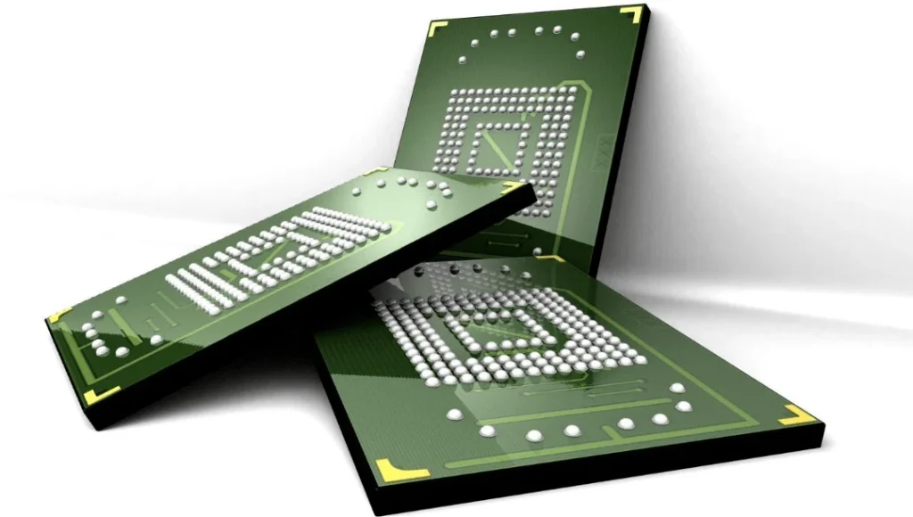
CSP Package Technical Concept and Classification
CSP Definition and Key Features
CSP refers to a package size close to the bare chip area, and the total package area does not exceed 1.2 times the chip area. This type of package retains the characteristics of the bare chip and provides package protection and interconnection capabilities. Compared with traditional BGA, QFN and other packaging forms, the core advantage of CSP is “almost no package boundary”, so the signal delay is low, the parasitic inductance is small, the package thickness is thinner, and it is more suitable for the modern electronic design needs of high-frequency, high-speed, and high-density integration.
Common CSP Types
FC-CSP (Flip-Chip CSP)
The chip is flipped and mounted on the substrate through micro-bumps to form a short-path package structure, which is suitable for high-frequency RF chips or RF front-end modules.
WLCSP (Wafer-Level CSP)
The solder balls are deposited directly on the chip at the wafer level and cut into packages: highly flat, typically less than 20×20mm, widely used in SD card controllers, Bluetooth chips, etc.
PoP-CSP (Package-on-Package CSP)
Stack multiple CSP packages together to achieve unified packaging of front-end processing and storage functions, suitable for smartphones and tablet products.
Comparison of CSP with other packaging forms
Compared with traditional BGA (ball grid array) and QFN (leadless package), the biggest advantage of CSP is its compact size, and the packaging area is usually no more than 1.2 times the chip itself. This means that CSP has almost no extra packaging boundaries, which shortens the signal transmission path, reduces parasitic parameters, and makes the signal integrity better, especially suitable for high-speed and high-frequency occasions.
Although BGA has good heat dissipation and I/O capabilities in structure, it is relatively large in size and is more suitable for main control chips or large-area packaging needs. QFN is widely used in general electronic products because of its relatively low manufacturing cost, but it does not perform as well as CSP in terms of multi-function integration and size compression.
Compared with composite packaging forms such as SiP (system-level package) or MCP (multi-chip package), although CSP is not as flexible and diverse in functional integration, it has the advantages of controllable cost, wide application range, high packaging efficiency, and has shown strong cost-effectiveness in the field of large-scale consumer electronics.
Detailed explanation of the manufacturing process
Although the CSP package has a compact structure, the manufacturing process is not simple at all. It combines multiple high-end process steps such as wafer-level process, micro-welding, precision mounting and packaging testing. The following is an analysis of the main manufacturing process of CSP Package.
Wafer processing and passivation protection
The packaging process of CSP starts with wafer processing. First, the back-end process (Back-End Process) is completed on the wafer, including wafer thinning (usually reducing the wafer thickness from the original 700μm to 200μm or even thinner) and covering the surface passivation layer to prevent the chip from being damp or affected by static electricity.
A bump welding area needs to be reserved on the passivation layer to ensure that the subsequent interconnection structure can reliably connect to the external circuit. Laser marking is usually added at this stage as an important identification point for subsequent traceability and automated processing.
Bump formation and redistribution layer (RDL) production
In order to achieve electrical interconnection between the chip and the package, CSP will form micro-bump pads (such as SnAgCu alloy) on the surface of the wafer. This step is usually completed by electroplating or evaporation. Subsequently, in order to match the solder ball layout of the package, a redistribution layer (RDL) needs to be constructed, that is, the original I/O of the chip needs to be rewired to the new solder joint location.
RDL is one of the key steps in CSP packaging. The material is generally copper or aluminum alloy, covered with a layer of polyimide as an insulating medium. This structure must ensure both electrical performance and good mechanical stability during thermal cycling.
Solder ball deposition and cutting separation
After completing the redistribution layer, the next step is to deposit solder balls on the pads of each CSP unit. These solder balls are generally attached by reflow soldering, melted and formed after heat treatment, and form a firm connection with the chip.
Subsequently, the entire wafer is cut (Dicing), and the wafer is divided into individual CSP packaging units by a high-precision cutting machine. This step has extremely high requirements for the tool, cutting path and speed control. If you are not careful, it may cause cracks or micro-defects in the corners of the chip, affecting the packaging yield.
Packaging test and sorting
After the cutting is completed, each CSP package needs to undergo functional and reliability tests to ensure that it can withstand future temperature stress, voltage shock and mechanical strain. The test items include:
Open/Short Circuit Detection (Open/Short Test)
High and Low Temperature Working Test (Thermal Test)
Signal Integrity Analysis (SI Test)
EMI Electromagnetic Interference Test
High Temperature and Humidity/Thermal Cycle Accelerated Aging Experiment
Qualified packages will be graded by sorting equipment, and unqualified products will be eliminated and the cause of the defect will be recorded for process optimization and quality traceability.
Mounting process adaptation
After the CSP packaging is completed, it will enter the SMT mounting stage. Due to its extremely small size and narrow solder ball pitch (Pitch can be as low as 0.4mm or less), the positioning accuracy and welding temperature control requirements of the mounting equipment are extremely high. Many high-end PCBA factories need to use automatic optical positioning (AOI), nitrogen reflow, 3D SPI and other equipment when processing CSP packaging to ensure uniform and reliable solder joints.
CSP’s core advantages and technical challenges
Maximizing space utilization and improving signal performance
The most significant advantage of CSP packaging is its small size and thin thickness. Since its packaging volume is only slightly larger than the bare chip itself, it can greatly save PCB board space, making it possible for terminal products to be lighter, thinner and more integrated. This feature makes it the preferred packaging solution for microelectronic products such as smartphones, wearable devices, and TWS headphones.
At the same time, due to the extremely short interconnection path, CSP has a natural advantage in high-frequency signal transmission. It can significantly reduce parasitic inductance and capacitance, thereby improving signal integrity (Signal Integrity), reducing signal delay, and helping high-performance computing chips to operate stably in complex systems.
Excellent thermal management and electrical performance
The compact structure of CSP also gives it certain advantages in heat conduction. Due to the short path between the chip and the outside, heat can be more directly extracted from the chip core. In addition, advanced CSP structures often combine designs such as thermal conductive base plates and copper column heat dissipation channels to improve the overall package heat dissipation efficiency.
On the other hand, the electrical performance of CSP is also better than that of traditional packages, especially in RF chips with frequencies above 1GHz. Its package impedance is controllable and parasitic interference is small, and it has basically become a standard in module applications such as power amplifier chips, Wi-Fi modules, and RF front ends.
Process challenges and reliability issues
Although CSP has many advantages, it also faces many challenges in the manufacturing and application process, especially in large-scale mass production and extreme usage scenarios, reliability issues are more prominent.
The first is thermal stress management. Due to the small package size and different expansion coefficients of the chip and substrate, stress concentration is very easy to occur during the thermal cycle, resulting in fatigue failure of the solder joints or microcracks.
The second is moisture sensitivity. CSP has an open structure, especially WLCSP (wafer-level CSP) packaging, which is very sensitive to humidity changes because the bare chip is exposed more. During high temperature and high humidity or wet reflow soldering, it is easy to produce a “popcorn” effect (that is, internal water vapor expansion destroys the packaging structure).
Another problem is the low tolerance for mounting. Due to the small size and narrow solder ball spacing, any mounting offset may cause failure problems such as open circuit, bridging, and cold soldering. This places extremely high demands on the precision control and process debugging capabilities of the SMT production line.
The dilemma of cost structure control
Although CSP has a cost advantage in theory due to its simplified structure and less packaging materials, its manufacturing process threshold is high, and the requirements for equipment, materials, and testing processes are significantly increased. Therefore, for small and medium-sized chip factories or packaging foundry companies, whether to invest in CSP production lines still needs to be considered in combination with product strategies, capacity planning, and customer needs.
In addition, although WLCSP eliminates the packaging substrate and plastic packaging process, it adds wafer-level processing and screening processes, and its yield control and process compensation capabilities become the key to affecting the overall cost.
Application fields and industry cases of CSP packaging
Consumer electronics: the backbone of the wave of lightweight and thinness
In the field of consumer electronics, CSP packaging technology has penetrated into almost all core components. From smartphones, tablets to smart watches, Bluetooth headsets and other portable devices, CSP has become the key to realizing the “smaller and stronger” product design concept due to its small size, flexible mounting and high functional density.
Taking smartphones as an example, most components such as RF modules, flash memory, audio chips, power management ICs (PMICs) use CSP packaging. Especially in 5G communication terminals, the number of frequency bands has increased significantly, the integration density is higher, and higher requirements are placed on the size control and electrical performance of RF front-end modules. CSP just meets this upgrade demand.
Wearable devices such as Bluetooth headsets and smart watches rely more on ultra-small packaging to make room for batteries, sensors and antennas. CSP packaging not only provides a space optimization solution, but also reduces the inductance and crosstalk problems between the device and the motherboard, and improves wireless performance and stability.
Automotive electronics: transition from edge to core control module
With the rapid development of smart cars and electric vehicles, CSP has gradually extended from the consumer electronics field to automotive-grade applications. CSP packaging has been widely adopted in subsystems such as in-vehicle entertainment systems, millimeter-wave radars, ADAS (advanced driver assistance systems) and TPMS (tire pressure monitoring systems).
Taking millimeter-wave radar chips as an example, CSP can provide excellent signal fidelity and heat conduction paths, while its small size facilitates system integration. In addition, CSP packaging has a lower tendency to electromagnetic interference (EMI) and can operate more safely in complex vehicle environments.
Although CSP faced reliability doubts when it entered the automotive electronics field, with the continuous maturity of the process and the optimization of packaging materials, more and more automotive parts manufacturers have begun to introduce it into the packaging of main control MCUs or micro sensors.
Industrial Internet of Things and Medical Equipment: Assisting High-Density Perception and Edge Intelligence
In the field of Industrial Internet of Things (IIoT), miniaturization and modularization have become core trends. Functional modules such as industrial control sensors, edge AI processing units, and industrial camera modules have extremely high requirements for space and energy consumption. CSP just meets its needs for size, electrical properties, connection speed and other aspects.
In addition, CSP’s high frequency and low interference characteristics make it widely used in medical imaging modules, implantable sensors, portable monitoring equipment and other scenarios. In these scenarios, the product’s requirements for packaging volume and stability are often strict, and CSP provides a very cost-effective solution.
Typical application cases: In-depth application of Apple and Qualcomm
As early as the iPhone 6 era, Apple used CSP packaging on a large scale in its Wi-Fi modules, audio ICs and sensor chips. Especially in recent generations of AirPods products, its highly integrated audio processing modules and Bluetooth modules rely on CSP to complete high-density stacking.
Qualcomm uses the Flip-Chip CSP structure in its RF front-end (RFFE) solution to integrate multiple filters and amplifiers in the same module. This solution combines size optimization and high-frequency transmission capabilities, making it an ideal choice for multi-band communications.
Future trends and technology evolution paths
As electronic technology continues to evolve, CSP packaging is also constantly breaking through its original boundaries. It is no longer limited to the single direction of “miniaturization”, but is expanding in multiple dimensions such as multi-functional integration, higher frequency support, and three-dimensional integration.
Fusion with advanced packaging technology
CSP is merging with more advanced packaging technologies. For example, the combination with system-level packaging (SiP) allows multiple functional chips to be stacked in a multi-layer structure in one package, meeting the dual demands for volume and performance in high-end smartphones and wearable devices.
In addition, CSP is also trying to merge with the chiplet architecture, packaging multiple heterogeneous chips in a short interconnection form through complementary layout, maximizing system performance and significantly improving production yield. In the future, the chiplet+CSP mode is expected to become the standard packaging method for high-performance computing and AI modules.
Wafer-level process moves towards extreme precision
WLCSP technology is evolving rapidly, and its solder ball size and wiring density are constantly improving. The solder joint spacing has been reduced from the early 0.5mm to 0.3mm or even lower. In order to ensure high reliability in extremely small packages, the wafer-level redistribution layer (RDL) process is shifting from traditional photolithography to eBeam precision mask and laser-assisted path wiring.
At the same time, new trends have emerged in CSP packaging materials, such as the use of low-dielectric-constant polymers as interposers and the introduction of copper pillar interconnect structures, which can further improve its heat resistance and electrical performance.
Intelligent manufacturing and packaging test automation
CSP production lines are accelerating the pace of automation. From wafer-level processes to packaging tests, AI detection and MES system management are being fully introduced to achieve full-process parameter visualization and yield traceability. The AI-assisted detection system can identify defects such as microcracks, solder ball anomalies, and pad detachment at the microscopic level, greatly improving quality control capabilities.
In the future, intelligent packaging factories will take CSP as the core to accelerate the high-end packaging industry from “experience manufacturing” to “data-driven” intelligent manufacturing.
Summary
CSP packaging has become an indispensable packaging form in modern electronic systems with its compact size, efficient signal transmission capability and superior cost structure. From smartphones to automotive radars, from industrial sensing to AI terminals, CSP is deeply embedded in every segmented scenario with strong adaptability and evolution potential.
However, the success of CSP does not only depend on its size advantage, but also on the huge and sophisticated manufacturing system, complex material selection, and deep control of reliability and performance behind it. With the integration of wafer-level processes, automated testing and heterogeneous packaging, CSP will play an increasingly critical role in cutting-edge fields such as 5G, the Internet of Things, and smart terminals.
For technicians, a deep understanding of CSP is not just about understanding a packaging form, but also a key step in gaining insight into the trend of miniaturization and intelligence in the electronics industry.