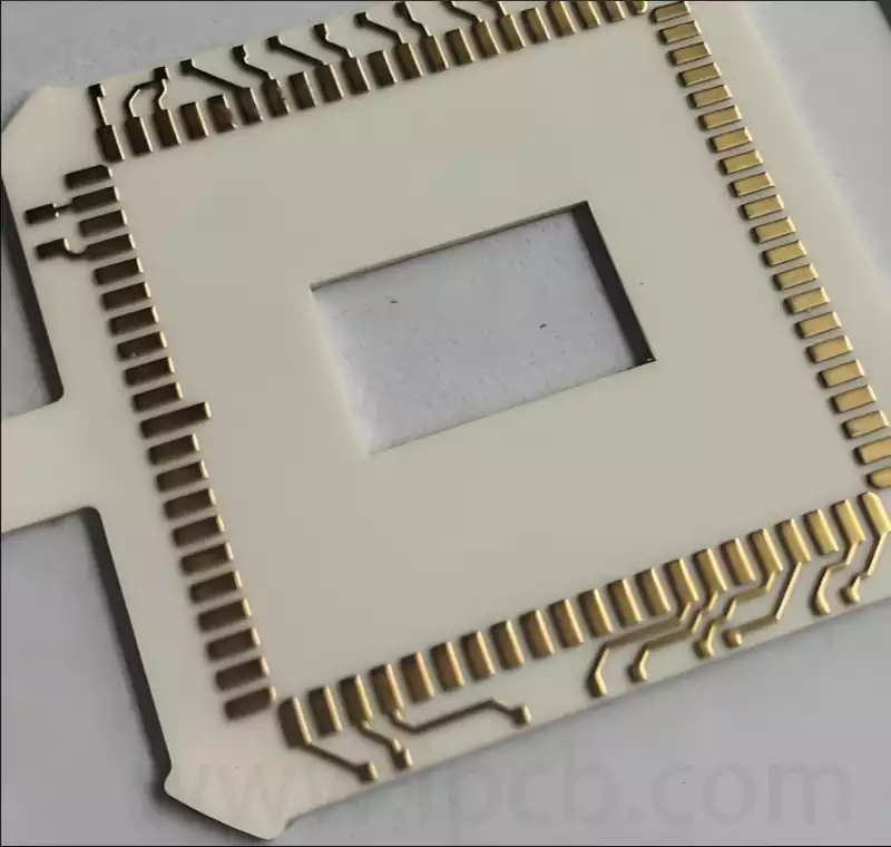
Ceramic circuit boards, owing to their high-temperature resistance and superior thermal conductivity, have progressively become the preferred substrate for high-power electronic components. However, their inherent ceramic properties pose significant challenges during the reflow soldering process—the slightest misstep can lead to substrate cracking and solder joint defects.
The fundamental difference between reflow soldering ceramic circuit boards and traditional FR-4 boards lies in the distinct physical properties of ceramic materials. These characteristics collectively form the core challenge in temperature curve control and dictate that conventional PCB soldering parameters cannot be applied.
The primary challenge is mismatched coefficients of thermal expansion (CTE). Common ceramic substrates like alumina, aluminium nitride, and silicon nitride exhibit CTE values of merely 4–7 ppm/℃, whereas lead-free solder (SnAgCu alloys) boasts a CTE of 20–24 ppm/℃—a disparity nearing threefold. During reflow soldering, the ceramic substrate, solder, and device leads heat up simultaneously yet expand at differing rates. Upon cooling, they contract asynchronously, generating persistent thermal stresses from this deformation disparity. If temperature fluctuations are too abrupt, stresses cannot dissipate promptly, leading to micro-cracks within the ceramic substrate. Though invisible to the naked eye, these cracks significantly degrade insulation properties and structural integrity, compromising product longevity.
The brittleness of ceramics and their poor thermal shock resistance further complicate temperature control. Unlike the toughness of FR-4 substrates, ceramic materials lack plastic deformation capability and are highly sensitive to abrupt temperature fluctuations. When the rate of temperature change exceeds the ceramic’s tolerance limit (typically ≤5℃/s), irreversible damage to the internal crystal structure may occur even without visible cracking. This is particularly critical for automotive-grade and industrial-grade ceramic circuit boards, which are highly susceptible to failure due to latent damage during subsequent high-low temperature cycling tests. Furthermore, while ceramic’s excellent thermal conductivity facilitates rapid heat transfer, it also readily leads to uneven surface temperatures, resulting in localised over-soldering or insufficient solder wettability.
The distinct properties of different ceramic materials necessitate tailored temperature profiles. Alumina ceramics, being cost-effective with moderate thermal conductivity (24–40 W/m·K), suit standard power applications. Designing reflow soldering profiles for alumina ceramic PCBs focuses on preventing thermal stress concentration. Aluminium nitride ceramics boast thermal conductivities of 170–230 W/m·K with a CTE closer to silicon chips, making them prevalent in high-frequency, high-speed applications. Temperature control for these boards must balance solder joint formation with substrate flatness. Silicon nitride ceramics offer the highest strength and superior thermal shock resistance, making them the preferred choice for automotive-grade IGBT modules. Temperature control must balance accommodating their high-strength requirements while ensuring solder metallurgical bonding quality.
Key Considerations for Reflow Soldering Profile Design of Ceramic Circuit Boards
The standard reflow soldering profile comprises four stages: preheating, temperature stabilisation, reflow, and cooling. For ceramic circuit boards, precise parameter calibration is essential. The core methodology involves ‘gradual heating, thorough temperature uniformity, precise peak control, and gradual cooling’. Parameter settings for each stage directly impact final soldering quality.
Preheat Stage
The primary objective of the preheat stage is to gradually elevate the board surface temperature, evaporate solvents within the solder paste, and release initial thermal stresses, thereby preparing the board for subsequent high-temperature phases. The preheat rate for ceramic circuit boards must be strictly controlled, ideally maintained at 2-3°C/s. During the initial 30 seconds, this rate should be further reduced to ≤2°C/s to prevent thermal shock caused by rapid heating in low-temperature zones.
The preheat endpoint temperature is typically set at 150-160°C, with a maximum temperature differential across the board surface of ≤8°C. This is particularly crucial for large ceramic circuit boards (>200mm) or component-dense products, where excessive temperature variations can lead to cumulative thermal stress during the subsequent constant-temperature phase. For moisture-absorbed ceramic circuit boards, it is advisable to conduct a preliminary baking treatment at 120°C for 4 hours. The preheating phase may be extended by 10-20 seconds to ensure thorough evaporation of internal moisture, thereby reducing the occurrence of solder void formation during the reflow stage. This also serves as a crucial prerequisite for optimising the temperature stabilisation time standards for ceramic circuit boards during reflow soldering.
Temperature Stabilisation Phase
The core objective of the temperature stabilisation phase (150–180°C) is to activate flux activity, remove oxidation layers from pads and component leads, and achieve uniform board surface temperature to prepare for solder melting. The holding time for ceramic circuit boards must be adjusted according to substrate type and dimensions. For standard alumina ceramic boards, a duration of 80–110 seconds is recommended. Due to their superior thermal conductivity, aluminium nitride and silicon nitride ceramic boards may have their holding time reduced to 70–90 seconds to prevent premature flux depletion and subsequent re-oxidation of pads.
During this stage, critical monitoring is required beneath BGAs and large-sized power components to ensure core temperatures exceed 150°C, otherwise solder wetting defects may occur. A common misconception is that ‘longer holding times yield better results’; in fact, excessive duration causes excessive flux evaporation, resulting in dull solder joint lustre and reduced mechanical strength. This is particularly problematic for fine-pitch pads on ceramic substrates, potentially leading to solder ball residue issues.
Reflow Stage
The reflow stage is critical for solder melting and intermetallic compound (IMC) formation. Parameter settings directly determine joint quality and ceramic substrate integrity, necessitating strict control of peak temperature and reflow duration.
Peak temperature must be set according to solder type and ceramic material properties. For lead-free solder (Sn-Ag-Cu alloys), a range of 245–255°C is recommended. The core principle for setting peak temperatures on ceramic circuit boards is empirical verification. Due to calibration deviations in reflow oven temperature zones, displayed temperatures may differ by 5-7°C from actual joint temperatures. Excessively high temperatures can cause ceramic substrate edge cracking and metal layer delamination, while insufficient temperatures result in incomplete solder melting and cold solder joints. For ceramic boards housing sensitive components, peak temperatures may be reduced to 240–245°C in conjunction with low-temperature-specific solder paste to prevent component performance drift. 265°C represents an absolute threshold; exceeding this causes irreversible damage to the ceramic substrate, constituting a critical control point for mitigating cracking risks during reflow.
The reflow duration (time spent above the solder melting point) should ideally be controlled at 20±5 seconds. For aluminium nitride ceramic circuit boards, this may be extended to 25-28 seconds to ensure thorough wetting of deep pads. However, exceeding 30 seconds is strictly prohibited, as it may cause excessive growth of the intermetallic compound (IMC) layer, rendering it brittle and prone to cracking during subsequent thermal cycling. The IMC layer thickness must be maintained between 2–4μm, as this range delivers optimal mechanical strength and fatigue resistance for solder joints. Both excessively thin and thick layers compromise the long-term reliability of ceramic circuit boards.
Cooling Phase
The core objective of the cooling phase is to control the rate of temperature reduction, minimising thermal contraction differences between the solder and ceramic substrate to prevent solder joint cracking and substrate damage. The cooling rate for ceramic circuit boards should be strictly controlled at 2-3°C/s. For automotive-grade ceramic circuit boards, the reflow soldering cooling rate must be further reduced to 1.5-2.5°C/s. A slow-cooling zone may be implemented: maintain a 3°C/s cooling rate above 220°C, reduce to 2°C/s below 220°C, and exit the oven below 100°C. This approach accommodates the stringent reliability requirements of automotive products.
Excessively rapid cooling poses a common hazard in ceramic PCB reflow soldering, akin to plunging red-hot glass into ice water. This induces instantaneous thermal stress, leading to ring-shaped cracking of BGA solder joints and micro-fractures in ceramic substrates. In some production scenarios, increasing cooling fan speeds to boost efficiency may shorten cycle times but substantially elevates the risk of subsequent failures. After cooling, ceramic circuit boards must be laid flat and allowed to rest undisturbed. Immediate movement or stacking is prohibited to prevent damage from external forces compounding thermal stress.
Optimising the reflow soldering temperature profile for ceramic circuit boards requires more than parameter adjustments; it demands avoiding common misconceptions and achieving full process coordination.
Common Misconception 1: Applying generic curves. Some production scenarios directly adopt FR-4 PCB curve parameters, disregarding the material differences of ceramics, leading to a sharp increase in substrate cracking rates. The correct approach is to establish a standard curve library based on ceramic material, size, and component type. Curves must be revalidated whenever changing materials or solder paste.
Misconception 2: Neglecting temperature probe placement. Positioning thermocouples solely on the substrate surface, without covering critical areas such as beneath BGAs or large components, leads to uncontrolled actual temperatures. Probes should be distributed across multiple points simulating real board layouts—at core solder joints, substrate edges, and beneath components. Critical products require curve verification through batch sampling.
Misconception Three: Neglecting environmental and incoming material impacts. PCB moisture absorption during rainy seasons and insufficient solder paste tempering can invalidate curve parameters, causing voids and cold solder joints. Control workshop temperature and humidity (23±3°C, humidity <60%), pre-bake incoming ceramic circuit boards, and temper solder paste for over 4 hours before use.
Full-process coordination is pivotal for temperature control. Temperature profiles must align with ceramic PCB design—incorporating stress relief slots to minimise thermal stress—and match material selection, choosing solder paste activity suited to substrate composition. Integration with pre-production treatments, such as baking and cleaning, reduces curve control complexity. Concurrently, establish process archives documenting curve parameters, equipment status, and failure cases to create a closed-loop optimisation system.
Optimising reflow soldering temperature profiles for ceramic circuit boards fundamentally involves precisely matching material properties with process parameters. Looking ahead, as ceramic materials gain widespread adoption in power electronics and automotive electronics, establishing standardised profile libraries and comprehensive process coordination mechanisms will become the core pathway for enhancing the soldering reliability of ceramic circuit boards.
