The laminate structure of RF PCB must consider not only the impedance of RF signal traces but also heat dissipation, current, components, EMC, structural integrity, and skin effect. When layering and stacking multilayer printed circuit boards, we typically adhere to the following fundamental principles:
A) Each layer of an RF PCB should feature a large ground plane. There should be no dedicated power plane; instead, the layers immediately above and below the RF routing layer should both be ground planes.
Even in mixed-signal boards, while digital sections may have power planes, the RF zone must still maintain extensive ground planes on every layer.
B) For double-sided RF PCB:
- Top layer: Signal layer
- Bottom layer: Ground plane
For four-layer RF PCB: - Top layer: Signal layer
- Second and fourth layers: Ground planes
- Third layer: Power and control lines
In special cases, some RF signal lines may run on the third layer. For multi-layer RF single boards, follow this pattern accordingly.
C) For RF backplanes, both top and bottom surface layers serve as ground planes. To minimize impedance discontinuities caused by vias and connectors, digital signals are routed on the second, third, fourth, and fifth layers.
Conversely, all stripline layers adjacent to the bottom plane function as bottom-side signal planes. Similarly, RF signal layers must be flanked by ground planes on both adjacent layers, with each layer featuring extensive ground planes.
D) For high-power, high-current RF pcb, place the primary RF links on the top layer using wide microstrip traces.
This facilitates heat dissipation, reduces energy loss, and minimizes conductor corrosion errors.
E) The power plane for digital sections should be positioned near the ground plane and arranged beneath it.
This utilizes the capacitance between the two metal planes as a smoothing capacitor for the power supply. Simultaneously, the ground plane shields distributed radiated currents on the power plane.
For RF double-sided boards, the top layer is typically the signal layer, while the bottom layer serves as the ground plane. For four-layer RF single boards, the top layer is the signal layer, the second and fourth layers are ground planes, and the third layer carries power and control lines. In special cases, the third layer may also carry some RF signal lines.
For RF backplanes, both top and bottom surface layers serve as ground planes. To minimize impedance discontinuities caused by vias and connectors, digital signals are typically routed on the second, third, fourth, and fifth layers. Other stripline layers near the bottom plane are bottom-side signal layers.
The power plane for digital sections should be positioned close to the ground plane and arranged beneath it. In RF pcb stackup design, particular attention must be paid to the layer stackup structure. Typically, the top layer of an RF pcb houses components and microstrip lines, the second layer features a large ground plane copper area, and the bottom layer consists of a solid copper plane directly contacting the enclosure ground plane. Intermediate layers carry signal traces. If multiple signal layers are required due to complexity, adjacent signal layers should be separated by ground planes. Signal layers should be routed perpendicular to each other—one layer primarily horizontal, the other primarily vertical.
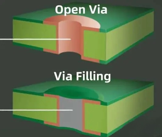
Additionally, RF PCB cannot utilize non-grounded via holes. Therefore, all network vias except ground vias must employ blind via design. For instance, in an eight-layer board design, to optimize stacking efficiency, the seventh layer is ideally designated for signal traces, resulting in numerous 1-to-7 blind vias. However, in actual manufacturing, such blind via designs may cause severe board warpage. To address this, back-drilling technology can be employed. This involves fabricating blind vias as through-holes, then drilling from the bottom upward to remove the copper plating between the seventh and eighth layers—without penetrating the seventh layer. For enhanced stability and to eliminate uncertainties, the hollowed-out section can be filled with resin.
Key Specifications for RF PCB Routing
Corner Treatment Specifications
When RF signal traces encounter right-angle corners, the effective trace width at the corner increases, causing impedance discontinuity and triggering signal reflection issues. Therefore, corners must be properly treated, with common methods including chamfering and rounding.
Fillet Requirements: The radius of the fillet must be sufficiently large, typically meeting R > 3W (where W represents the trace width).
Chamfer Application: Chamfers are suitable for smaller bends and can be used up to frequencies of 10GHz.
Strip Line Routing Requirements
Occasionally, RF signals must traverse the intermediate layers of a PCB high-frequency RF PCB, most commonly routing from the third layer. In such cases, the second and fourth layers must form complete ground planes, creating an eccentric strip line structure. To ensure the integrity of the strip line structure, the following specific requirements apply:
Prohibition of Ground Plane Gap Crossing: RF strip lines are strictly prohibited from crossing gaps between upper and lower ground planes.
Edge Distance Requirements: The edges of the stripline must maintain a minimum distance of 3W from the edges of the upper and lower ground planes. Within this 3W width, no ungrounded vias are permitted.
Ground Plane Edge Distance: It is recommended that the distance between the edge of the ground plane and the stripline edge be greater than or equal to 1.5W or 3H (where H represents the total thickness of the dielectric layers above and below the stripline).
Ground Plane Copper and Ground Via Treatment: Striplines on the same layer require ground plane copper coverage. Ground vias must be added on the ground plane, spaced less than λ/20 (where λ is the signal wavelength) and arranged uniformly. The edges of the ground copper foil must remain smooth and flat; sharp burrs are strictly prohibited.
High-Power Signal Transmission Treatment: When transmitting high-power signals, to avoid excessive narrowing of the 50-ohm line width, the copper layers on both reference planes above and below the stripline region should be etched away. The etching width must exceed five times the total dielectric thickness of the stripline. If the line width still fails to meet requirements, the adjacent second reference plane above and below should be further etched away.
Microstrip Line Layout Requirements
When routing RF signals on the top layer of an RF PCB, the plane layer beneath the RF signal must form a complete ground plane, creating a microstrip line structure. To ensure the integrity of this microstrip structure, the following specific requirements apply:
Prohibition of Gap Crossing: RF signal traces are strictly prohibited from crossing gaps between second-layer ground planes.
Distance Requirement to Shielding Walls: Maintain a minimum distance of 2W (where W is the trace width) between microstrip lines and shielding walls.
Edge Distance Requirement: The edges of the microstrip line must maintain a minimum distance of 3W from the edge of the underlying ground plane. Within this 3W width, no ungrounded vias are permitted. Additionally, the edges of the ground copper foil must be smooth and flat; sharp burrs are strictly prohibited. It is recommended that the distance between the edge of the ground copper foil and the edge of the microstrip line be greater than or equal to 1.5W width or 3H width (where H denotes the thickness of the microstrip substrate dielectric).
Non-coupled microstrip line treatment: Non-coupled microstrip lines on the same layer must be wrapped with ground copper foil. Ground vias should be added on the ground foil, spaced less than λ/20 (where λ is the signal wavelength) and arranged uniformly and neatly.
Strict adherence to RF PCB laminate and routing specifications is fundamental to creating high-performance RF circuits. Attention to every detail ensures stable circuit operation and lays a solid foundation for diverse RF applications.