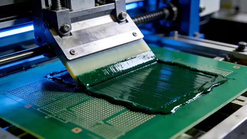
In the field of PCB manufacturing, screen printing refers to the process technology whereby conductive pastes, solder resist inks, character inks and other materials are precisely transferred onto the surface of the PCB substrate through a screen stencil using a squeegee under pressure. Following curing, this forms specific patterns or functional layers. Its core principle originates from traditional ‘rubber-stamping’ techniques, yet through modernised equipment and material advancements, it achieves micron-level precision control. This enables adaptation to the full spectrum of PCB production requirements, spanning rigid to flexible boards and standard boards to HDI boards.
Distinct from other printing technologies, PCB screen printing exhibits three significant characteristics: Firstly, stencil dependency, where the aperture pattern of the screen stencil directly determines the shape of the printed layer, serving as the core vehicle for precision control; Secondly, pressure-driven operation, wherein squeegee pressure forces paste through mesh apertures onto substrates, with pressure intensity directly influencing layer thickness and uniformity. Thirdly, curing necessity, as printed paste requires thermal or UV curing to form stable functional layers. These three characteristics collectively constitute the irreplaceable technical foundation of screen printing within PCB manufacturing.
Core Process Flow of PCB Screen Printing
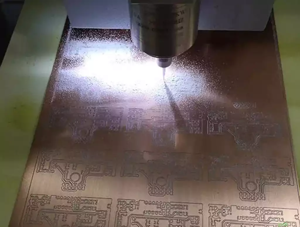
1.Screen Stencil Fabrication
Screen Base Selection: Base materials comprise polyester mesh and stainless steel mesh. Polyester mesh offers superior flexibility and lower cost, making it suitable for printing solder mask and character layers on standard rigid PCBs. Stainless steel mesh provides high strength and stable mesh openings, capable of withstanding high-viscosity paste extrusion, and is the preferred choice for printing conductive traces on HDI boards and flexible PCBs. Mesh count selection must align with printing requirements: higher counts yield finer apertures and enhanced precision. Standard PCBs typically use 200-300 mesh screens, while HDI boards necessitate 350-450 mesh high-count screens.
Photoresist coating: Apply photoresist uniformly across the screen substrate surface. Coating thickness must be determined by printing layer requirements: 15-25μm thickness is required for solder mask printing to ensure post-curing protective layer thickness compliance; character layer printing requires only 5-10μm thickness to prevent excessive thickness affecting component assembly. This process requires a specialised coating machine to ensure uniform photoresist thickness without bubbles or pinholes.
Film Alignment and Exposure: Precisely align the film containing the PCB pattern with the coated screen before placing it in an exposure unit for ultraviolet irradiation. Light-transmitting areas on the film cause the photoresist to cure, while non-transmitting areas remain uncured. Registration deviation in this step must be controlled within ±10μm; otherwise, printed pattern misalignment may cause circuit short-circuits or pad blockage issues.
Development and Curing: The exposed screen is immersed in developer solution, where uncured photosensitive resin dissolves to form apertures matching the film pattern. Subsequently, it undergoes secondary curing in an oven to enhance the photoresist layer’s adhesion and abrasion resistance, ensuring the stencil remains durable during mass production. Currently, high-end PCB factories have adopted laser cutting to replace traditional photolithography, directly cutting precise apertures into the metal mesh. This achieves alignment accuracy of ±5μm while eliminating the need for film and development steps, significantly reducing stencil production lead times.
2.Pre-press Preparation
Paste Preparation and Mixing: Select the appropriate paste according to the printing type — silver paste/copper paste for conductive circuit printing, insulating solder mask ink for solder mask printing, and high-adhesion character ink for character layer printing. Two preparatory steps are required before paste application: Firstly, viscosity adjustment. Modify viscosity according to ambient temperature, maintaining conductive pastes between 8000–15000 cP and solder mask inks between 5000–8000 cP. Add thickener for insufficient viscosity, or dedicated thinner for excessive viscosity. Secondly, thorough stirring is essential to prevent pigment settling within the paste, which could cause uneven colouration and reduced performance in the printed layer. Conductive paste requires stirring for 15-20 minutes, while solder mask ink requires 10-15 minutes.
PCB substrate pre-treatment: Clean and dry the PCB substrate prior to printing to remove surface dust, grease, and moisture. Dust causes pinholes in printed layers, grease reduces paste adhesion to the substrate, and moisture forms bubbles during curing. Plasma cleaning equipment is recommended for pre-treatment, as it efficiently cleans surfaces while enhancing surface activity and improving paste adhesion.
Equipment alignment calibration: Mount the fabricated screen stencil onto the screen printing machine. Utilise a CCD vision alignment system to precisely register the stencil pattern with the PCB substrate’s reference points, maintaining alignment deviations within ±10μm. Simultaneously adjust the printing gap (distance between screen template and substrate). For rigid PCBs, set the printing gap to 1–3 mm; for flexible PCBs, reduce this to 0.5–1 mm to prevent substrate deformation during printing.
3.Formal Printing
Squeegee Pressure and Speed: The squeegee serves as the driving force for paste transfer, with its pressure and speed directly determining print layer thickness and uniformity. Insufficient pressure prevents adequate filling of mesh apertures, resulting in inadequate layer thickness; excessive pressure causes paste to spread under compression, leading to widened traces or blurred characters. Parameters require differentiation for various PCB types: Standard rigid PCBs: Doctor blade pressure 0.2–0.6 MPa, speed 50–100 mm/s. Flexible PCBs: Pressure reduced to 0.1–0.3 MPa, speed slowed to 30–50 mm/s to prevent damage to the flexible substrate. Squeegee material selection must also align with requirements: polyurethane squeegees offer good elasticity, suitable for most PCB printing; metal squeegees possess high hardness, ideal for thick-film printing with high-viscosity pastes.
Paste replenishment and recovery: During printing, continuously replenish paste onto the screen stencil to ensure consistent mesh aperture filling. After printing, promptly recover residual paste from the stencil, seal it for storage and reuse to minimise raw material wastage.
Release control: Upon printing completion, the screen stencil must separate rapidly from the PCB substrate. This separation must occur at a uniform and stable speed to prevent paste adhesion to the stencil, which causes rough edges in the printed layer. Modern screen printing machines incorporate automated release control systems that automatically adjust release speed and angle based on paste characteristics and substrate type.
4.Curing Process
Conductive paste curing: Employ a high-temperature oven for curing. Silver paste curing temperature ranges from 120–150°C with a holding time of 30–60 minutes. Copper paste curing temperature must be elevated to 180–200°C to ensure thorough sintering of copper particles, forming conductive pathways. The curing process must strictly control the heating rate to prevent rapid solvent evaporation from the paste, which could cause bubbles or pinholes.
Solder resist ink curing: This is a two-step process of ‘pre-baking + final baking’. First, pre-bake at 80°C for 30 minutes to slowly evaporate the solvent from the ink. followed by a final bake at 150°C for 60 minutes to fully cure the solder resist ink, forming an insulating protective layer. Some high-end PCBs utilise UV-curable solder resist ink, which cures within 30-60 seconds under ultraviolet light exposure, significantly reducing production cycles and enhancing mass production efficiency.
Character ink curing: Employ a low-temperature curing method, maintaining temperatures between 80-100°C for 20-30 minutes to prevent discolouration or peeling of character ink due to excessive heat. UV curing is equally applicable to character ink, offering higher curing efficiency.
5.Post-processing and inspection
Post-processing operations: Includes deburring, trimming, and cleaning to remove excess paste from printed layer edges and clear curing residues from the PCB surface, ensuring no component mounting issues arise from poor pin contact.
Quality inspection: Utilises AOI (Automated Optical Inspection) equipment for comprehensive testing of printed layer thickness, uniformity, and pattern accuracy. Inspection criteria include: whether circuit edges are smooth and burr-free; whether characters are clearly legible and spaced ≥0.2mm from pads; and whether conductive traces exhibit short circuits or open circuit defects. Non-compliant PCBs must be promptly reworked or scrapped to prevent their entry into subsequent processes and avoid greater losses.
The Core Role of Screen Printing in PCB Manufacturing
1.Conductive Circuit Formation
For specialised categories such as flexible PCBs and thick-film PCBs, screen printing serves as the direct method for forming conductive circuits. By printing conductive paste onto the surface of flexible substrates and curing it at high temperatures, conductive pathways are formed, replacing the etching process used in traditional rigid PCBs. This process offers advantages by eliminating complex photolithography, development, and etching steps, preventing damage to flexible substrates from etching solutions. It also enables printing thick-film circuits on substrate surfaces to meet high-current transmission requirements. For instance, conductive circuits in flexible PCBs for new energy vehicles are achieved through screen-printed silver paste, delivering stable conductivity and withstanding over 100,000 bending cycles.
2.Solder Mask Formation
The solder mask serves as an insulating protective layer covering the PCB surface, with over 90% of PCB solder masks formed via screen printing. Its core functions include preventing circuit oxidation, avoiding solder joint short circuits, and enhancing the PCB’s resistance to moisture, heat, and corrosion. Through screen printing, solder mask ink can be precisely applied to non-pad areas, while pad locations are accurately left uncoated, ensuring reliability during component soldering. High-quality solder mask printing enables PCBs to withstand over 500 hours of salt spray testing without oxidation and operate reliably for years in high-temperature, high-humidity environments.
3.Character Layer Formation
The character layer comprises component location, polarity, and model identification markings on the PCB surface. It serves as critical reference for PCB assembly, maintenance, and traceability, with its formation entirely dependent on screen printing. Character printing must meet the requirements of being ‘clear and legible, with strong adhesion and no peeling’. By selecting high-adhesion character inks and employing precise registration printing, it is ensured that characters remain sharp and intact during subsequent soldering and cleaning processes. For high-density HDI boards, character printing must accommodate the layout of minute components. High-mesh-count screen stencils are utilised to ensure characters are compact and clear, without obscuring critical pads.
Common Defects in Screen Printing and Resolution Strategies
Solder Mask Pinholes and Air Bubbles
Causes: Insufficient solvent evaporation in ink, inadequate curing temperature, moisture or dust on substrate surface.
Resolution: Extend pre-baking time to 30-40 minutes; increase final baking temperature to 150-160°C. Plasma clean substrates prior to printing; select solder mask inks with low solvent content.
Rough Circuit Edges
Causes: Insufficient mesh count, inadequate paste viscosity, excessive squeegee pressure.
Solutions: Replace with high-mesh screens (350-450 mesh); add thickener to increase paste viscosity; reduce squeegee pressure to appropriate levels.
Character blurring and peeling
Causes: Excessive squeegee pressure causing character diffusion, insufficient curing temperature, poor character ink adhesion.
Solutions: Reduce squeegee pressure to 0.2–0.3 MPa; adopt a staged curing process of ‘80°C pre-bake + 120°C final bake’; select high-adhesion character ink compatible with the substrate.
Pad Blockage
Causes: Screen stencil aperture deviation, excessive paste flow, misalignment.
Solutions: Re-manufacture high-precision screen stencils; select thixotropic solder resist ink (higher thixotropy reduces ink flow); employ CCD vision alignment systems to enhance positioning accuracy.
Uneven Layer Thickness
Causes: Inconsistent squeegee pressure, poor screen template flatness, uneven paste distribution.
Solutions: Adjust squeegee pressure to uniform levels; replace with flat screen templates; ensure even paste distribution across the template prior to printing.
Screen printing, as a ‘traditional process’ in PCB manufacturing, appears deceptively simple yet possesses profound technical depth. As PCBs evolve towards higher density, greater reliability, and flexibility, screen printing technology continues to advance. The application of intelligent vision alignment systems, automated paste control equipment, and laser-cut stencil technology is propelling this traditional craft towards ‘high precision, intelligent operation, and environmental sustainability’.