SMD LED is small and highly efficient light emitting diodes (LEDs) that are commonly used in electronic products as indicator lights or display backlights. Compared to conventional LEDs, SMD LEDs have higher density and better energy efficiency. They are named “SMD” because they can be affixed directly to printed circuit boards, saving space and improving productivity.
Positive and negative polarity distinction
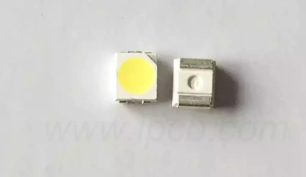
The positive and negative terminals of SMD LEDs can be distinguished by the shape of the package, its color, and the location of the pins. Usually, the positive terminal of a SMD LED is connected through a longer pin, while the negative terminal is connected through other shorter pins. In addition, some manufacturers will be printed on the negative pin next to the “+” or “-” and other signs, to facilitate the user to connect correctly.
Composition of smd beads
All LEDs are similar in light emission, only the appearance of the bracket is not the same. smd SMD beads are composed of: bracket, wick, IC.
- The semiconductor wafer consists of two parts, one part is a P-type semiconductor, in which holes dominate, and the other end is an N-type semiconductor, in which electrons dominate on this side.
- These two semiconductors are connected, P-type semiconductor inside the hole will drift to the N area, with the free electrons there, the same, N-type semiconductor inside the electrons will drift to the P area, with the hole there, so that, due to the loss of holes in the P area is negatively charged, the loss of electrons in the N area and is positively charged, the formation of an electrostatic field hindering the drift of electrons and holes between them, the formation of a “P-N junction”.
- When the current through the wire to act on this wafer, the electron will be pushed to the P region, in the P region of the electron with the hole complex, and then it will be in the form of photons to send out energy, which is the principle of LED light-emitting.
- And the wavelength of light, that is, the color of light, is formed by the P-N junction material decision. White LED because the ic chip emits blue light excitation coated with yellow phosphor, blue and yellow = white!
SMD lamp beads encapsulation process
LED encapsulation process: process
- Cleaning step: use ultrasonic cleaning PCB boards or LED bracket, and drying.
- Mounting steps: the bottom electrode in the LED core ready to expand after the silver glue, the expansion of the core placed on the piercing table, under the microscope with a piercing pen will be installed one by one in the circuit board or LED the corresponding pads, followed by sintering to make the silver glue curing.
- Pressure welding step: aluminum wire or gold wire welding machine will be connected to the electrode on the LED core for the current injection lead. LED directly mounted on the PCB, generally using aluminum wire welding machine.
- Encapsulation step: through the dispensing of glue, epoxy LED core and welding line protection. Dispensing on the PCB substrate, the shape of the cured gel has strict requirements, which is directly related to the brightness of the finished backlight. This process will also take on the task of pointing phosphor.
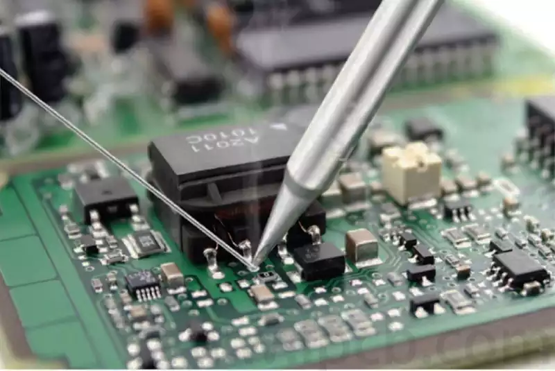
- Soldering step: If the backlight is SMD-LED or other encapsulated LEDs, the LEDs need to be soldered to the PCB board before the assembly process.
- Film cutting step: die cutting various diffusion films and reflective films required for the backlight source with a punch.
- Assembly step: according to the drawing requirements, the various materials of the backlight source manual installation of the correct position.
8.Testing step: Check whether the photoelectric parameter of the backlight source and the uniformity of the light are good. - Packaging steps: the finished product according to the requirements of the packaging, warehousing
How to produce led light beads
LED lamp beads of the entire production process, divided into epitaxial wafer production, chip production, lamp bead packaging, the entire process reflects the level of modern manufacturing technology in the electronics industry, LED manufacturing is a set of a variety of technology fusion, is a high-tech products for the lighting purposes of the LED knowledge mastery is also needed to understand the LED lamp beads are produced.
1.LED epitaxial wafer production process:
LED epitaxial wafer growth technology mainly uses organic metal chemical phase deposition method (MOCVD) production of synthetic materials with semiconductor properties, is the raw material for the manufacture of LED chips
- LED chip production process:
LED chip is manufactured using epitaxial wafer, is to provide the LED lamp bead package device, is the key to the quality of LED lamp beads. - LED bead production process:
LED bead packaging is based on the requirements of the use of LED beads, the chip is encapsulated in the corresponding bracket to complete the LED bead manufacturing process, LED packaging to determine the cost-effectiveness of LED beads, LED lamps and lanterns is the key to the quality of the product.
SMD LED features
Small size
High assembly density, small size and light weight of electronic products, the volume and weight of only about 1/10 of the traditional plug-in components.
Strong vibration resistance
High reliability, strong vibration resistance, low solder joint defect rate
Low cost
Easy to realize automation, improve productivity, reduce costs up to 30% ~ 50%
Applications
- Active component (LED) or passive component (backlight)
- Lighting
- Color temperature or color system
- Efficiency
- Spectrum
SMD LED, with their miniature size, efficient energy utilization, and convenient mounting methods, are becoming indispensable components in electronic products.