What is solder mask layer? Soldermask, the soldering surface layer used to assemble electronic components, is usually made of a solderable material with a specific surface treatment and chemical composition that allows the components to be easily attached to the PCB.
The surface of the soldermask is usually coated with a thin layer of solder paste, a mixture of solder and flux. When the electronic component is placed on the PCB, the solder paste adheres to the component’s pins and to the PCB’s solder mask. The solder paste is then melted by heat, soldering the component pins to the PCB’s solder mask.
It should be noted that the thickness and solderability of the solder resist layer has an important impact on the quality of PCB soldering, if the solder resist layer is too thin or too rough, it may lead to poor soldering or poor electrical connection, if the solder resist layer is too thick or too smooth, it may lead to bridging or short-circuiting between the pins of the components.
So in terms of soldermask, must pay attention to the thickness of the soldermask and surface treatment.
Soldermask in the control of reflow soldering in the soldering defects is very important, PCB designers should minimize the pad around the spacing or air gap.
While many process engineers would rather have a welding mask that separates all pad features on the board, the pin spacing and pad size of close-pitch components will require special consideration. While undivided weld mask openings or windows on a four-sided qfp may be acceptable, controlling solder bridges between component pins may be more difficult. For bga’s weld mask, many companies offer a weldingmask that does not touch the pads but covers any features between the pads to prevent tin bridging. Most surface mount PCBs are covered with a weldingmask, but the application of the weldingmask, if it is thicker than 0.04mm, may affect the application of solder paste. Surface mount PCBs, especially those using closely spaced components, require a low profile photo resist layer.
Job Fabrication
Solder mask material must be applied by either a liquid wet process or a dry film overlay. Dry film soldermasks are supplied in thicknesses of 0.07-0.1mm and can be suitable for some surface mount products, but they are not recommended for close pitch applications. Few companies offer dry film thin enough to meet close-pitch standards, but a few companies offer liquid photopolymerized soldermasks. Typically, the opening of the welding mask should be 0.15mm larger than the pad, which allows for a 0.07mm gap around the edge of the pad. Low-profile liquid photopolymerized soldermasks are economical and are often specified for surface mount applications, providing precise feature sizes and clearances.
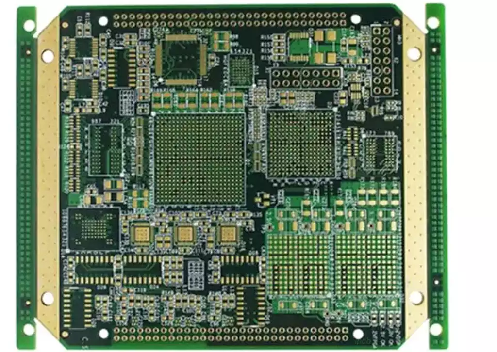
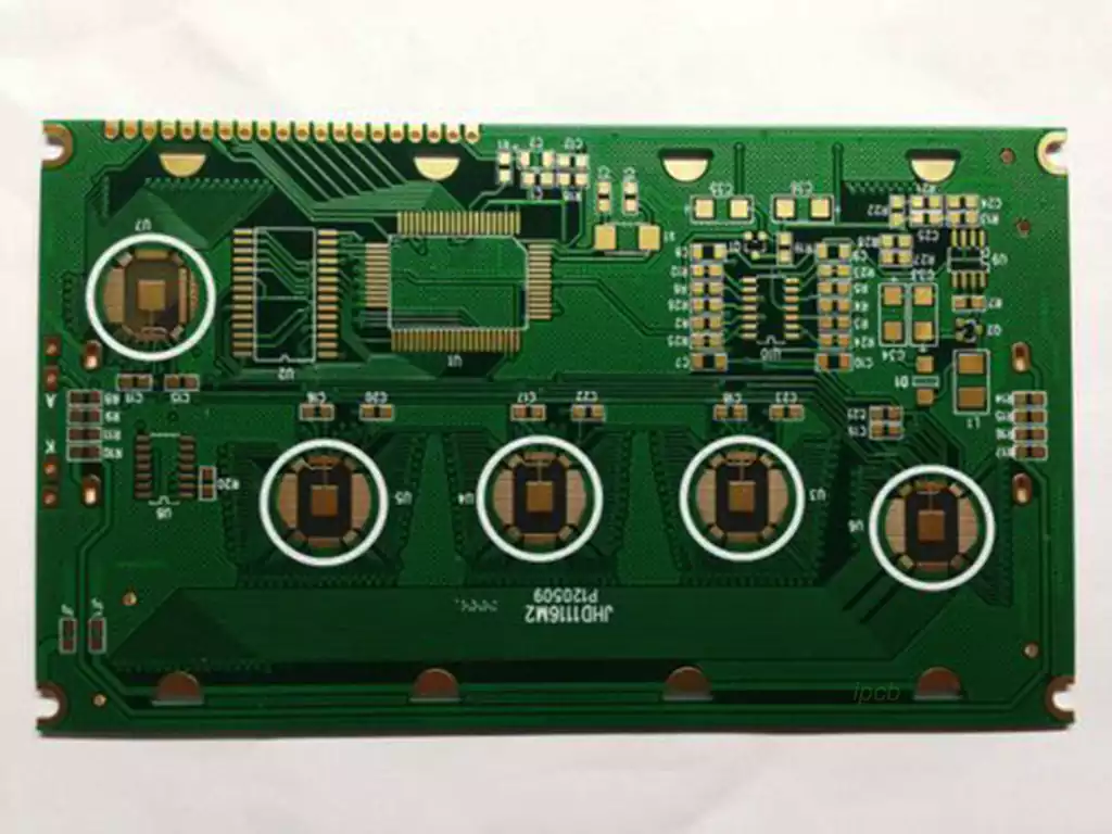
Solder mask layer prevents conductive solder bridging between various electronic components. In essence, it thwarts short circuits. The different PCB solder mask layers are as follows.
Top and Bottom Masks: The electronic engineer knows about the various openings. He knows what has been added by ink, epoxy or film techniques. He is then able to solder the component pins on the board with the assistance of a confirmed orientation. It is also possible to notice conductive trace patterns on the top of the board. Call these the top stares. Lower down are the bottom masks.
Epoxy Liquid: For an inexpensive pick, pick an epoxy liquid. Thermoset polymers are used in a variety of applications. Screen printing is a printing technique. It utilizes a woven mesh to support the ink resist pattern. The mesh creates an open area for the ink to travel.
Liquid inks for photographic imaging: We supply soldermask as an ink formulation. The ink can be sprayed into the PCB and then the pattern can be exposed and developed. It is important to note that the process is utilized as well as the liquid ink formulation. This requires a clean environment free of contaminants and particles. One is able to remove it after exposing it to UV light. This is done by means of a high-pressure water spray called a developer.
The dry film can be imaged photographically: the solder mask layer is applied by vacuum lamination. After development, you can create openings and solder the parts to copper pads. In addition, tin is applied to maintain the copper circuits. The dry film is then removed.
The main purpose of the solder mask layer:
- Prevent oxidation:
Oxidation is a common problem with metals. Since copper traces are metal, they are very susceptible to oxidation. Oxidization on copper traces affects their ability to conduct current, and worse, it can lead to short circuits and ultimately damage the board. Therefore, use a solder mask layer to seal the copper traces from the atmosphere and prevent oxidation. - Prevent solder bridges:
Solder bridges are accidental solder flows that occur on the outside of a component during soldering. These bridges will form connections with nearby alignments or pads, thus creating a short circuit path. Solder bridges can be highly present in PCBs with SMD components where there is little or no space between the component and the alignment. Applying a solder resist layer to the PCB surface will prevent solder from flowing out of the designated area, thus eliminating the possibility of forming a solder bridge. - Aesthetics:
Finally, soldermask gives the PCB an aesthetic appearance. Green is the most commonly used color, but there are other available colors such as black, red, yellow, and blue.
The flux layer is used for SMD packaging and corresponds to the SMD component pads. In SMT processing is usually used a steel plate, the PCB corresponds to the component pads on the place of punching holes, and then the steel plate on the solder paste, circuit board in the steel plate under the time, the solder paste leaks down, it is just about every pad can be stained with solder, so usually the flux layer can not be larger than the actual pad size, it is best to be smaller than or equal to the actual pad size. Need for the level and surface-mounted components are almost the same, the main need for the following elements:
1.BeginLayer: ThermalRelief and AnTIPad than the rules of the actual size of the pad 0.5mm larger
2.EndLayer: ThermalRelief and AnTIPad should be 0.5mm larger than the actual size of the regular pads
3.DEFAULTINTERNAL: Intermediate layer
PCB flux layer and solder resist layer difference
Both layers are on the tin soldering with, does not mean a tin, a green oil; but:
- Soldermask layer means that the whole piece of soldermask on the green oil to open the window, the purpose is to allow soldering;
- By default, there is no soldermask layer of the area are to be on the green oil;
- The flux layer is used for SMD packaging.
Solder mask layer and flux layer as a double protection layer of PCB welding, not only to ensure the accuracy and reliability of welding, but also to enhance the overall performance and aesthetics of the circuit board, is an indispensable key technology in the modern electronics industry.