Solder resist material is a fine polymer coating used on printed circuit boards (PCBs) whose primary function is to protect the copper surface of the board from oxidation and the formation of unwanted electrical connections (i.e., solder bridges) during the soldering process. The application of soldermask is critical to improving the reliability of the board and preventing short circuit events.
Common solder resist material:
Top and Bottom Masks
The use of this type of soldermask is common among electronic engineers. They use this type of solder to identify openings in the solder layers. The layering of this type of soldermask is usually done using film or epoxy technology.
Epoxy Liquid Solder Mask
This is one of the less expensive soldermask options because it is a polymer that you can easily screen print on the PCB. Screen printing is a printing method where you have to use a woven mesh to hold the ink pattern.
Liquid Solder Resist / Photo Imaging Solder Resist
This solder resist material is usually the superior of the four. By nature, it is a mixture of two different liquid components. As a result, it has a longer shelf life than other solder resists. Additionally, it is versatile in its application, which means you can use a variety of techniques to apply this solder resist type.
Dry Film Photo Imaging Solder
This type of soldermask is great for high-density circuit boards. Since the film is dry, it is less likely to escape from the holes. In addition, vacuum lamination techniques should be used when applying dry film.
Different types of soldermask have unique physical properties and application scenarios, and engineers need to choose the right material for a specific project.
Solder resist material is mainly used on circuit boards to protect copper traces from contamination and oxidation during the soldering process. They are widely used in mass production and processes such as wave soldering and reflow techniques to ensure the functionality and stability of circuit boards.
The key features of soldermasks include preventing solder short circuits, reducing oxidation and corrosion, and providing good insulation properties. They effectively avoid solder bridges caused by closely spaced pads and ensure the reliability of each solder joint. In addition, soldermasks are resistant to the effects of the external environment, such as moisture and dust.
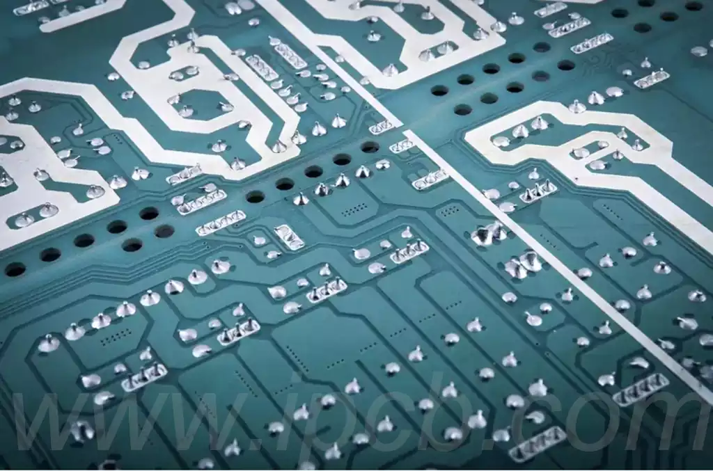
Typically, soldermasks are green in color, but they can also come in other colors such as white, blue, or black to meet different design needs. This choice of color is not only for aesthetic reasons, but many engineers choose a specific color to differentiate between prototype and production boards.
The manufacturing process for soldermask consists of several steps including cleaning, coating, pre-hardening, exposure, development and final hardening. Each step plays a critical role in the reliability and performance of the board, so strict process standards and technical requirements must be followed to ensure the quality of the final product.
- Cleaning the board
The first step in manufacturing soldermask is to clean the board. This step is designed to remove surface dirt and oxides in order to provide a smooth and dry surface for subsequent processes. - Applying Soldermask
After cleaning the solder resist material, the board is loaded into the coater for soldermask application. The thickness of the coating is adjusted according to the functional requirements of the board, the service area and the thickness of the board to ensure uniformity and reliability of the coating. - Pre-hardening
After coating, the soldermask is pre-hardened. This stage is not a complete hardening, but a preparation for subsequent development and exposure to ensure that the coating is firm to a certain extent for subsequent processes. - Imaging and Exposure
Next, a transparent film with an image of the circuit is covered with the board and exposed to UV light. This process hardens the areas covered by the film, while the uncovered areas remain unhardened. It is important to ensure that this process is aligned to avoid subsequent problems with exposure of unspecified copper foils. - Developing Stage
After UV exposure, the board is placed in a developer that removes the unhardened soldermask to reveal the designated copper pads. - Final Hardening and Cleaning
Finally, final hardening of the soldermask is performed to ensure that it fully adheres to the PCB surface.Once this is done, the board is cleaned to ensure that the surface is free of any contaminants in preparation for subsequent assembly and surface treatment.
Selection of suitable solder resist material in the PCB manufacturing process is critical, the main criteria include the material’s film-forming properties, thickness, color, high-temperature performance and cost.
1.Film-forming properties
Solder resist material must have a good film to ensure that the application process can form a uniform and strong protective layer. This standard is usually based on the U.S. civilian standard IPC-SM-840C for identification, to ensure that the material can effectively cover the substrate after curing.
2.Thickness
The thickness of the soldermask is another key criterion,which usually depends on the thickness of the copper traces on the PCB.Generally,a soldermask of approximately 0.5 mils is required to cover the copper traces to ensure effective prevention of solder bridge formation.
In addition, the thickness of the solder resist material is specified for different grades of PCBs, with no limit on the thickness for grade 1 products and minimum thickness requirements for grade 2 and 3 products.
3.Color
Color selection is also important,usually commonly used color is green. This is because green ink provides good contrast during inspection and examination, making it easy to detect defects and also providing a better visual effect. Different colors of soldermask will also vary in visual effect and functionality, according to the specific needs of the choice.
4.High temperature resistance
In the production process often need to withstand high temperatures, so its high temperature performance is very important. Soldermask needs to meet standards such as UL94V-0 to ensure that the stability and integrity of the environment can still be maintained at high temperatures. This performance directly affects the reliability and service life of the PCB board.
- Cost
Finally, the cost is the choice of solder resist material can not be ignored.For manufacturers, cost-effective soldermask material is more desirable. Under the premise of quality assurance, should consider the procurement cost of various materials and their impact on the performance of the final product.
Solder resist material plays an indispensable role in the manufacture of printed circuit boards. They effectively protect the copper surface,prevent oxidation and solder short circuits, to ensure the reliability and stability of the board.Choosing the right material is critical to realizing high-quality and high-performance electronics.