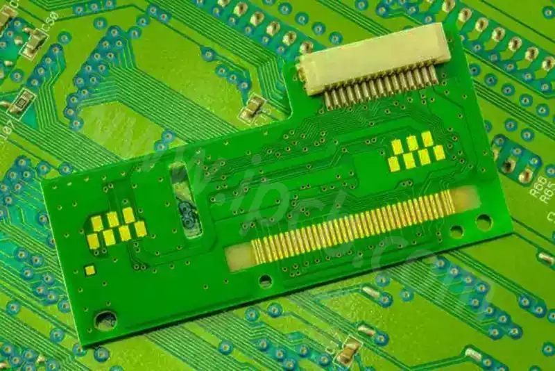
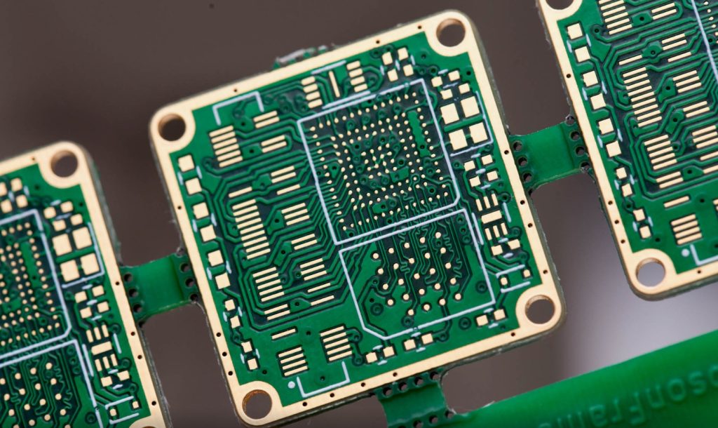
The optical module PCB serves as a pivotal component for achieving electro-optical conversion, playing a crucial role within communication systems. It facilitates the transformation of electrical signals into optical signals, or vice versa, thereby ensuring efficient, long-distance data transmission through optical fibres.
When designing optical module PCBs, multiple factors must be thoroughly considered, including signal integrity, thermal management, and electromagnetic compatibility. Only through such comprehensive consideration can stable and reliable operation of the optical module be guaranteed within high-speed, high-density data transmission environments.
Transmission Distance of Optical Modules
The transmission distance of optical modules is categorised into short-range, medium-range, and long-range. Generally, distances of 2 km or less are considered short-range, while those of 30 km or more are classified as long-range.
In practical applications, the achievable transmission distance is constrained primarily by signal attenuation and dispersion occurring during fibre propagation.
Attenuation
Refers to the gradual weakening of optical signal intensity during transmission through the fibre medium. Measured in dB/km.
Primary sources of optical signal loss include fibre material absorption loss, scattering loss, bending loss, and connector/joint loss. Typically, single-mode fibre exhibits lower attenuation than multi-mode fibre.
Dispersion
Refers to the phenomenon where light pulses broaden due to differing propagation speeds of signals at varying frequencies or modes within the fibre, leading to signal distortion. It is measured in ps/(nm·km). Dispersion causes adjacent pulses to overlap, increasing bit error rates and thereby limiting the fibre’s maximum transmission rate and unrepeatered transmission distance.
Key Technologies and Materials for Optical Module PCBs
The rapid advancement in transmission speeds—from early 1G/10G to current 400G/800G and even 1.6T—imposes increasingly stringent demands on PCB materials. To minimise signal loss and distortion during transmission, high-frequency, high-speed optical module PCBs require materials with extremely low dielectric constant (Dk) and dielectric loss factor (Df). Furthermore, as optical module dimensions continue to shrink—such as in miniaturised modules like SFP and QSFP-DD—increasing numbers of integrated chips are required within their compact footprints. Consequently, employing blind/buried via and microvia technologies to enhance routing density becomes paramount to meet these miniaturisation demands.
The manufacturing process for optical module PCBs involves numerous critical steps, including engineering data processing, material selection and cutting, lamination, drilling, and plating. Engineering data processing constitutes a vital stage, involving meticulous impedance calculations and simulations to provide precise guidance for subsequent manufacturing. Furthermore, employing high-precision LDI equipment during production minimises errors inherent in traditional processes, thereby ensuring product quality.

Optical Module PCB Design Requirements
As the cornerstone of high-speed optoelectronic conversion, the design quality of an optical module’s internal PCB directly impacts the module’s overall performance, reliability, and cost. As optical module speeds advance towards 400G, 800G, and even 1.6T, coupled with the stringent industrial-grade reliability demands of 5G applications, PCB design faces unprecedented challenges. This necessitates engineers possessing robust theoretical knowledge of Signal Integrity (SI) and Power Integrity (PI), alongside meticulous, systematic consideration across layout, routing, material selection, and thermal management.
Key Considerations for High-Speed Signal Integrity Design
Within ultra-high-speed optical modules, electrical signals traverse PCBs at rates reaching 56G PAM4, 112G PAM4, or higher, with frequencies extending into the millimetre-wave band. At such elevated frequencies, PCB traces cease to behave as ideal conductors, instead exhibiting the characteristics of distributed-parameter transmission lines. Any design oversight—such as impedance mismatch, crosstalk, or loss—can cause severe signal distortion, leading to eye diagram closure failure, a sharp increase in bit error rate, and ultimately rendering the module inoperable. Consequently, high-speed signal integrity design is paramount in optical module PCB design.
Rigorous Impedance Control and Low-Loss Design Strategies
Impedance control forms the bedrock of high-speed signal integrity design. Within optical modules, the signal path from gold fingers to DSP chips and onward to optical engines (TOSA/ROSA) must maintain continuous and stable characteristic impedance to prevent signal reflection. For differential signals, impedance is typically required to be controlled within the range of 100Ω ± 10%. However, numerous ‘traps’ exist in practical PCB design that cause impedance discontinuities, such as gold fingers, chip pads (BGA), coupling capacitor pads, and via structures.
To overcome these challenges, designers must implement a series of meticulous optimisation measures. For instance, in a study of 25G ONU optical modules, researchers observed that the cross-sectional area at gold fingers and coupling capacitor pads far exceeded the signal trace width, resulting in low characteristic impedance. To address this, they employed a ‘reference plane excavation’ technique. This involves locally removing material from the reference ground plane beneath the pads. By increasing the distance between the signal and the reference plane, parasitic capacitance is reduced, thereby enhancing the impedance in this region to match the transmission line impedance. Beyond impedance control, minimising signal transmission loss is equally critical. Signal loss primarily encompasses conductor loss and dielectric loss, which are closely related to signal frequency, PCB material properties (such as Df value), and copper foil roughness. For high-speed optical modules, it is essential to select low-loss PCB materials and optimise routing design. Measures such as employing wider line widths, shorter trace lengths, and avoiding unnecessary via transitions can effectively reduce insertion loss.
Crosstalk Suppression and Differential Pair Optimisation Methods
In high-speed, high-density PCB designs, crosstalk between signal lines is unavoidable. Crosstalk refers to the phenomenon where energy from one signal line couples onto an adjacent line, causing interference. Within optical modules, differential signalling is the primary transmission method. Consequently, coupling within differential pairs and crosstalk between them are critical design considerations.
To suppress crosstalk, the ‘3W principle’ must first be adhered to: the spacing between adjacent signal traces should be at least three times the trace width. For differential pairs, maintaining constant spacing and coupling ensures robust common-mode rejection capability. During layout, high-speed differential traces should be kept sufficiently distant from other traces, particularly clock signals. During routing, avoid excessively long parallel runs whenever possible. Where unavoidable, insert ground planes between parallel traces for isolation. Optimising differential pair routing is also critical. Differential pairs should preferably be routed on the same layer to minimise impedance discontinuities and crosstalk caused by vias. If layer changes are unavoidable, both signal lines of the differential pair must change layers simultaneously. Symmetrical ground vias should be placed near the layer-change vias to provide a continuous return path for the signals.
Power Integrity (PI) and Ground Plane Design Considerations
Power Integrity (PI) holds equal importance to Signal Integrity. In high-speed digital circuits, switching operations within chips generate transient currents. Should the impedance of the Power Distribution Network (PDN) be excessively high, this induces voltage fluctuations (power noise) on the supply lines, thereby compromising chip functionality.
To establish a low-impedance PDN, pcb design must employ a multilayer board structure with dedicated, independent power and ground planes. These planes should be tightly coupled to form a planar capacitor, providing a low-impedance return path for high-frequency transient currents. Numerous decoupling capacitors must be placed near the chip’s power pins to filter out power noise across different frequencies. The selection and placement of these capacitors require careful calculation and simulation, typically employing combinations of capacitors with varying capacitance values and packages to cover a broader frequency range. Ground plane design is particularly critical. A complete, continuous ground plane provides the optimal return path for signals, effectively reducing EMI and crosstalk. In optical module PCB design, unnecessary segmentation of the ground plane should be avoided. Where segmentation is unavoidable (e.g., to isolate analogue and digital grounds), ensure signal traces do not cross the segmentation boundaries. Failure to do so will result in discontinuous return paths, causing severe EMI issues.
Optical module PCB design must address multiple technical considerations and confront numerous challenges. Only through meticulous control and continuous optimisation can its stable performance in the communications field be assured.


