The physical characteristics of millimetre-wave signals render their transmission far more fragile than that of lower-frequency signals, forming the core premise for their reliance on high-density interconnect(HDI) technology. Compared to traditional low-frequency electromagnetic waves, millimetre waves exhibit three inherent limitations, each posing stringent challenges to printed circuit board interconnect techniques.
1.Severe signal attenuation necessitates minimising transmission paths. Millimetre waves possess extremely short wavelengths, rendering them susceptible to obstruction by the atmosphere, water, and structures during transmission. Concurrently, they exhibit pronounced skin effect – where current concentrates within an extremely thin surface layer of conductors – causing signal attenuation to increase exponentially with rising frequency. Data indicates that millimetre waves in the 60GHz band attenuate to less than one-thousandth of their initial strength after transmitting 100 metres through air. This necessitates minimising signal transmission paths in millimetre wave devices. High-density interconnect technology achieves this through meticulous circuit layout and interlayer connections, compressing transmission distances between chips, antennas, and RF modules to the absolute minimum, thereby substantially reducing signal loss.
2.Sensitivity to signal interference necessitates stringent electromagnetic compatibility (EMC) requirements. The ultra-wide bandwidth of high-frequency millimetre-wave signals makes crosstalk between adjacent signal channels highly probable. Concurrently, the extremely high component density within millimetre-wave devices, where diverse signals intertwine, further exacerbates the risk of electromagnetic interference. Failure to meet EMC standards not only reduces signal transmission rates but may also trigger equipment malfunctions. High-density interconnect technology effectively isolates different signal channels through minute line width/spacing designs and rational grounding/shielding structures. This enhances electromagnetic compatibility, ensuring pristine transmission of millimetre-wave signals.
3.Sensitivity to phase noise compromises signal integrity. Core millimetre-wave functions such as phased array beamforming demand stringent phase consistency. Even minute phase noise deviations cause beam steering errors, degrading communication quality and detection accuracy. Conventional interconnect technologies, with their unstable line impedance and imprecise interlayer connections, readily introduce phase noise. High-density interconnect (HDI) technology, through high-precision laser drilling and uniform electroplating processes, achieves stable impedance matching and precise interlayer interconnections. This safeguards the phase consistency of millimetre-wave signals, laying the foundation for realising core device functionality.
Three Key Roles in Overcoming Millimetre-Wave Challenges
High-density interconnect (HDI) technology transcends mere ‘circuit densification’. Through precision routing, multi-layer stacking, and micro-via techniques, it precisely addresses the high-frequency demands of millimetre-wave devices across three dimensions: transmission pathways, electromagnetic isolation, and integration efficiency. This makes HDI the core solution to overcoming inherent limitations.
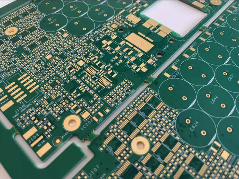
- Shortening transmission paths to reduce signal attenuation. A core advantage of high-density interconnect technology lies in achieving exceptionally fine circuit layout. Conventional PCBs typically feature line widths/spacing exceeding 100μm, whereas HDI can reduce these parameters to below 50μm, with high-end products achieving precision as fine as 20/20μm. This fine-pitch routing enables ‘close-proximity interconnections’ between chips, antennas, and RF modules within millimetre-wave devices. It reduces signal transmission paths from the conventional centimetre scale to the millimetre scale, substantially diminishing signal attenuation during transmission. For instance, in 77GHz millimetre-wave radar, implementing high-density interconnect technology reduced the transmission path between the RF chip and antenna by 60%, while lowering signal attenuation by over 40%, effectively extending the radar’s detection range.
- Optimising electromagnetic isolation to enhance signal purity. High-density interconnect(HDI) technology establishes an efficient electromagnetic shielding system through multi-layer stacking structures and rational grounding design. On one hand, the multilayer stacking arrangement segregates different signal types (e.g., RF signals, digital signals, power signals) across distinct layers, preventing direct interference between them. On the other hand, the implementation of continuous ground copper foil between signal layers forms a ‘signal layer-ground layer’ shielding structure. This effectively blocks external electromagnetic interference while preventing internal millimetre-wave signals from radiating outward. Furthermore, high-density interconnects featuring minute vias (diameters as low as 0.1mm or less) enable precise inter-layer grounding, further enhancing electromagnetic compatibility. Within the RF units of 5G millimetre-wave base stations, the adoption of high-density interconnect technology reduced signal crosstalk by 50%, ensuring stable base station communications.
- Enhancing integration efficiency to meet device miniaturisation demands. The core functionality of millimetre-wave devices often relies on extensive component integration. For instance, addressing the limited transmission range of millimetre-wave signals necessitates large-scale phased array antennas, integrating hundreds of antenna elements within confined spaces. In autonomous driving 4D millimetre-wave radar systems, multiple modules—including RF transceiver chips, signal processing chips, and power management chips—must be integrated concurrently. High-density interconnect (HDI) technology substantially increases component integration density by accommodating more traces and vias within limited PCB area. Compared to conventional PCBs, HDI boards achieve 3-5 times greater integration density, enabling extensive component interconnection within minimal space to meet millimetre-wave equipment’s miniaturisation and lightweighting requirements. For instance, the millimetre-wave communication module in high-end smartphones, utilising high-density interconnect technology, has seen its volume reduced by 70%, successfully achieving integrated packaging with the handset.
From autonomous driving to satellite interconnectivity, from 5G high-end terminals to industrial detection, millimetre-wave devices across diverse fields rely on high-density interconnect(HDI) technology as a core enabler. The demands of these practical applications further validate the necessity of high-density interconnect for millimetre-wave equipment.
In autonomous driving, 77GHz and 79GHz millimetre-wave radars serve as core perception devices, with their performance directly determining driving safety. Such radars require integrating multiple RF channels, antenna units, and signal processing modules within extremely compact spaces, while demanding ultra-low transmission latency and exceptional phase consistency. The adoption of high-density interconnect(HDI) technology has increased the number of RF channels in radars from the traditional four to sixteen, tripling detection accuracy while reducing volume by 50%. This enables seamless integration into confined spaces such as vehicle front bumpers and rear-view mirrors. Currently, high-density interconnect technology is universally employed in millimetre-wave radars for mainstream Level 3 and above autonomous vehicles.
Within the 5G millimetre-wave communications domain, the antenna-in-unit (AAU) of base stations integrates numerous antennas and RF chips, imposing stringent demands on circuit board integration and signal transmission performance. Conventional PCBs cannot meet the interconnection requirements of large-scale antenna arrays. High-density interconnect(HDI) technology, through multi-layer stacking and fine-pitch routing, enables the integration of large-scale antenna arrays with 64 or even 128 channels. Simultaneously, the low-loss characteristics of high-density interconnect ensure stable transmission of 5G millimetre-wave signals, enhancing base station coverage and communication speeds. Globally, the RF units of 5G millimetre-wave base stations universally employ high-density interconnect circuit boards, forming the core guarantee for achieving high performance in base stations.
In the field of satellite interconnectivity, the millimetre-wave band is pivotal for achieving high-speed communication between satellites and ground stations. Satellite equipment faces stringent weight and volume constraints while simultaneously requiring resilience against the extreme conditions of space, such as high temperatures, low temperatures, and intense radiation. High-density interconnect (HDI) technology not only enhances the integration density of satellite millimetre-wave communication modules, reducing their size and weight, but also improves the environmental resilience of circuit boards through optimised materials and processes. For instance, in low-Earth orbit satellite millimetre-wave communication modules, the adoption of HDI technology has reduced module weight by 40% and volume by 50%, while enabling stable operation across an extreme temperature range of -55°C to 125°C.

Why do conventional interconnect technologies fail to meet millimetre-wave equipment requirements? The core issue lies in their inability to match the high-frequency characteristics of millimetre waves in terms of line precision, integration density, and signal transmission performance. Traditional PCBs feature larger line widths/spacings, resulting in longer signal paths and significant attenuation. Their low integration density cannot accommodate the demands of large-scale component integration. Furthermore, poor electromagnetic isolation leads to severe signal crosstalk, compromising signal purity during transmission.
Taking traditional FR-4 PCBs as an example, their line widths/spacings typically exceed 100μm, resulting in extended signal transmission paths. At the 77GHz millimetre-wave frequency band, signals degrade by over 1.5dB per centimetre of transmission, rendering them unsuitable for millimetre-wave device requirements. Concurrently, conventional PCBs feature large via diameters (typically exceeding 0.3mm), limited via counts, and low integration density, precluding the integration of large-scale phased array antennas. Furthermore, inadequate grounding designs in traditional PCBs result in poor electromagnetic isolation, with signal crosstalk levels reaching below -30dB, severely compromising millimetre-wave signal transmission quality.
Compared to conventional interconnect technologies, high-density interconnect (HDI) achieves a qualitative leap across multiple critical metrics. Trace width/spacing can be reduced to 20/20μm, substantially shortening signal transmission paths; via diameters can be minimised below 0.1mm, increasing via density by 5-10 times and significantly enhancing integration density; Through multi-layer stacking and precise grounding design, electromagnetic isolation is substantially enhanced, reducing signal crosstalk to below -60dB and ensuring pristine millimetre-wave signal transmission. These advantages make high-density interconnect technology the sole viable option for millimetre-wave devices.
As millimetre-wave technology advances towards higher frequency bands (e.g., above 100GHz), demands on high-density interconnect technology continue to escalate. To meet future requirements for millimetre-wave devices, this technology is evolving towards greater precision, lower loss, and enhanced reliability.
On one front, line fineness is continuously improving. Future millimetre-wave devices will utilise higher-frequency signals, necessitating further refinement in line precision. The industry has commenced development of high-density interconnect technology featuring line widths/spacing of 10/10μm. Advanced processes such as Semi-Additive Process (SAP) and Modified Semi-Additive Process (MSAP) enable the fabrication of finer traces. This ultra-fine routing further shortens signal transmission paths, reduces attenuation, and accommodates the demands of higher millimetre-wave frequencies.
Concurrently, low-loss materials are seeing broader application. Signal loss remains a core challenge for millimetre-wave devices; beyond shortening transmission paths, employing low-loss materials constitutes a critical solution. Future high-density interconnect circuit boards will increasingly utilise low-loss FR-4 substrates, PTFE substrates, and similar materials. These exhibit lower dielectric loss factors (Df), effectively reducing dielectric loss during signal transmission. For instance, PTFE substrates possess a dielectric loss factor of merely 0.002, substantially lower than the 0.02 typical of conventional FR-4 substrates. High-density interconnect circuit boards employing this material can achieve a further reduction in signal attenuation exceeding 30%.
Furthermore, reliability design continues to be refined. As millimetre-wave devices find increasingly diverse applications, demands on circuit board reliability grow ever more stringent. Future high-density interconnect technologies will enhance circuit board environmental resilience, radiation resistance, and mechanical strength through optimised electroplating processes, additional line protection layers, and radiation-resistant materials. This ensures stable operation of millimetre-wave devices in extreme conditions.
The integration of millimetre-wave equipment with high-density interconnect(HDI) technology is not a fortuitous technical choice, but rather an inevitable outcome of precisely matching the demands of high-frequency signal transmission with the capabilities of interconnect technology. The inherent limitations of millimetre-wave technology necessitate reliance on high-density interconnect (HDI) techniques to achieve short-path transmission, efficient electromagnetic isolation, and high integration density. Conversely, the continuous evolution of HDI technology provides the core foundation for millimetre-wave devices to advance towards higher frequency bands, greater miniaturisation, and enhanced reliability.
With the deepening development of 5G and accelerated deployment of 6G, the application scope of millimetre-wave devices will continually expand, driving sustained growth in demand for high-density interconnect(HDI) technology. For electronics manufacturers, gaining a profound understanding of the core advantages of high-density interconnect technology and mastering its compatibility logic with millimetre-wave devices is key to enhancing product competitiveness. Looking ahead, ongoing innovation and breakthroughs in high-density interconnect technology will further enhance the performance of millimetre-wave devices and broaden their application scenarios, injecting fresh momentum into the development of the electronics industry.


