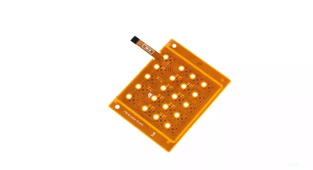
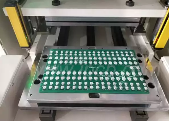
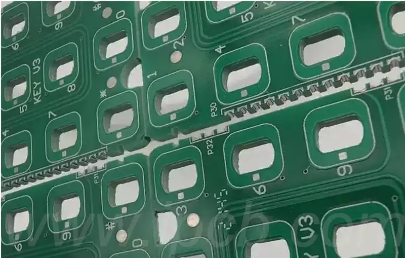
Rigid Flex PCB Stackup refers to the combination of rigid PCBs and flexible PCBs to form a stack of circuit boards with a multi-layer structure. This technology combines the stability of rigid PCBs with the flexibility of flexible PCBs, allowing for better bending and folding properties while maintaining structural strength.
Typical flexible circuit boards or rigid-flexible circuit boards look simple. However, its nature requires several additional steps to be performed during the build process. The starting point for any rigid-flex board is always a single or double-sided flexible layer. Manufacturers can start with pre-laminated flex with foils, or they can start with an uncoated PI film, which is then laminated or copper plated for initial cladding. Laminated films require a thin layer of adhesive, while non-adhesive overlays require a “seed coat” of copper. This skin layer is initially implanted using vapor deposition techniques (i.e., spray plating) and provides the key to chemically deposited copper plating. The drilling, plating, and etching steps for such single- or double-sided flexible circuits are much the same as those for a typical double-sided core in a rigid circuit board.
Several laminated structures are commonly used for FPCs
Single-sided boards
A single-sided copper-clad board material is used to create a flexible circuit board with a single layer of conductors, which is covered with a protective film or overcoat after the circuit is completed.
Ordinary double-sided board
The use of double-sided copper-clad materials in the double-sided circuit is completed, and then a layer of protective film is added to each side to become a circuit board with two layers of conductors.
Substrate Generation Single-Sided Boards
Using two layers of single-sided copper-layered material with a windowed adhesive in the middle, the board is pressed together in a localized area and the two layers are separated in a localized area, resulting in a board with a high degree of flexural performance in the layered area.
Multilayer Boards
Using single-sided copper-layered boards and bonding adhesive as the basic material, the boards are pressed together several times to form a multilayer conductor structure using a process similar to that used to generate double-sided boards from a substrate, and can be designed as a localized layered structure for the purpose of achieving a high degree of flexural performance.
Rigid-flex PCBs
Rigid-flex PCBs are composed of rigid and flexible substrates selectively laminated together in a compact structure with metallized holes to form conductive connections. Each rigid-flex printed board has one or more rigid areas and one or more flex areas.

Advantages of Rigid Flex PCB Stackup Technology:
Increased board integration. Through the multi-layer stacking design, more circuit components and lines can be integrated into a smaller space, thus reducing the size and weight of the whole system, providing the possibility of miniaturization and lightweighting of electronic products.
Enhanced board reliability. Due to the combination of rigid and flexible PCBs, the circuit boards have better stability and durability when subjected to external forces or vibrations, improving the service life and reliability of the products.
Rigid and flexible PCB stacking technology also has excellent electrical properties. The design of the multi-layer structure makes the circuit board’s conductivity more superior and signal transmission more stable, providing strong support for high-speed data transmission and low noise applications.
Just Rigid Flex PCB Stackup technology with its unique advantages, for the electronics manufacturing field has brought new opportunities for development. With the continuous progress of technology and the expansion of application areas, it is believed that the rigid-flexible PCB stacking technology will play an even more important role in the future to promote the continuous innovation and development of the electronics industry.


