The principle of multilayer PCB design is to lay out different circuit components according to their functions and locations, and then connect them through wires. During the design process, various factors need to be considered, such as the selection of parameters for components such as resistors, capacitors, inductors, etc., the routing of signal wires, and the layout of power supply wires. In addition, factors such as electromagnetic compatibility and thermal management need to be considered to ensure the stability and reliability of the board.
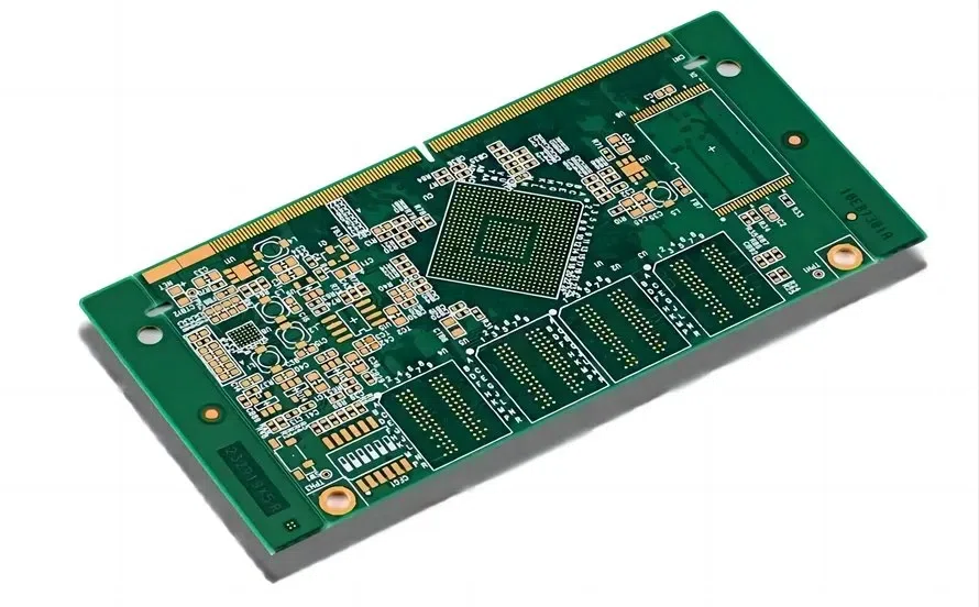
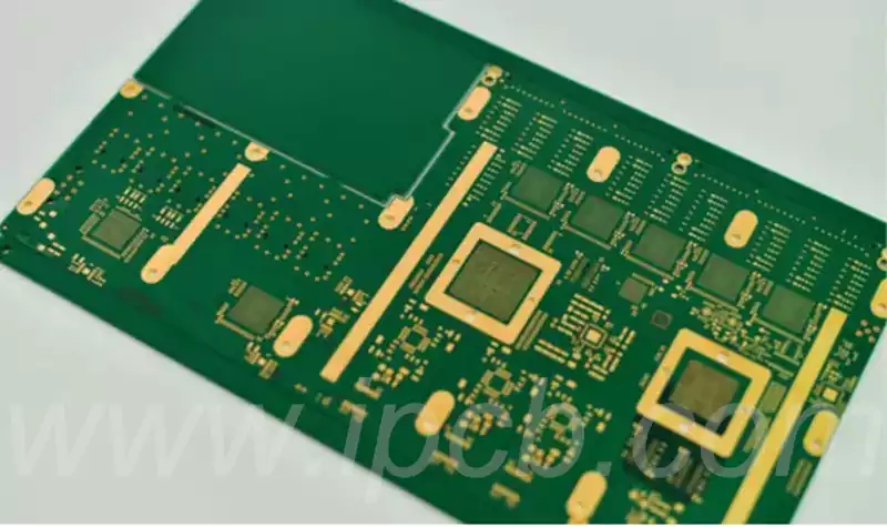
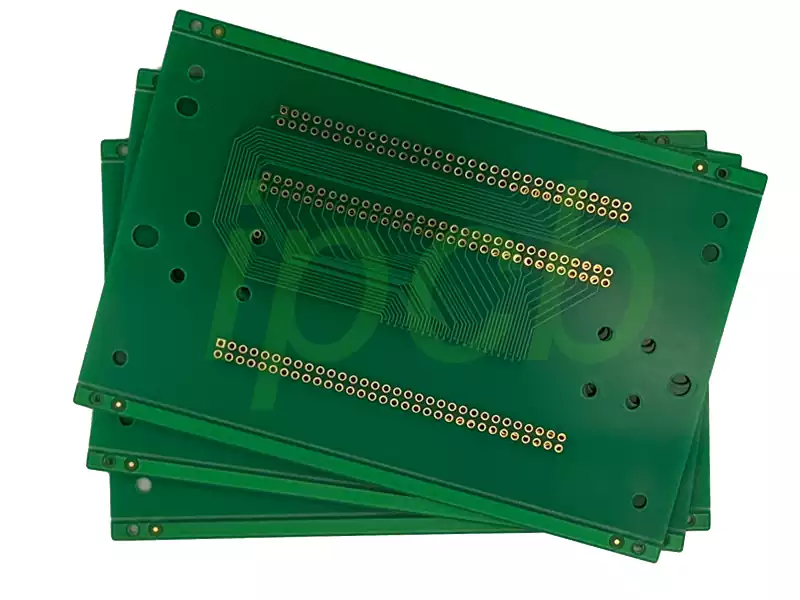
Multilayer pcb design
EDA365 Electronics Forum believes that when the laminate is designed, the layers should be kept symmetrical, and it is best to have an even number of copper layers, if it is not symmetrical, it is easy to cause distortion. Multilayer board wiring is carried out according to the circuit function, in the outer layer wiring, the requirements of more wiring in the welding surface, less wiring in the component surface, which is conducive to the maintenance of the printed circuit board and troubleshooting.
In terms of alignment, it is necessary to separate the power, ground and signal layers to reduce the interference between power, ground and signal. The lines of the two adjacent layers of printed circuit boards should be as perpendicular to each other as possible or go diagonal, curved lines, not parallel lines, in order to reduce the interlayer coupling and interference of the substrate.
Board shape, size, layer determination
The shape and size of the printed board must be based on the product structure of the whole machine. EDA365 e-Forum reminds us that, from the production process point of view, it should be as simple as possible, generally for the length and width ratio is not too disparate rectangular, in order to facilitate the assembly of the improved production efficiency and reduce labor costs.
In terms of the number of layers, it must be based on the requirements of the circuit performance, board size and line density. For multilayer printed circuit boards, four-layer boards, six-layer boards are most widely used.
The layers of the multilayer board should be kept symmetrical, and it is best to have an even number of copper layers, i.e., four, six, eight, etc.. Because of the asymmetric lamination, the board surface is prone to warpage, especially for surface mounted multilayer boards, more attention should be paid.
Component location and placement direction
Component location, placement direction, first of all, should be considered from the circuit principle, catering to the direction of the circuit. Placement of reasonable or not, will directly affect the performance of the printed circuit board, especially high-frequency analog circuits, the location of the device and placement requirements, obviously more stringent.
Therefore, engineers in the beginning of the layout of the printed circuit board, the overall layout of the decision, should be a detailed analysis of the circuit principle, the first to determine the location of special components (such as large-scale ICs, high-power tubes, signal sources, etc.), and then arrange the other components, as far as possible, to avoid possible interference with the factors.
On the other hand, the overall structure of the board should be considered from the printed circuit board to avoid uneven and chaotic arrangement of components. This not only affects the aesthetics of the printed board, but also brings a lot of inconvenience to the assembly and maintenance work.
Wire cloth layer, wiring area requirements
In general, multi-layer printed circuit board wiring is carried out according to the circuit function. In the outer layer wiring, the requirements of more wiring in the welding surface, the component surface less wiring, which is conducive to the maintenance of the printed circuit board and troubleshooting.
Fine, dense wires and easily disturbed signal lines are usually arranged in the inner layer. Large areas of copper foil should be more evenly distributed in the inner and outer layers, which will help reduce the warpage of the board, but also make plating on the surface to obtain a more uniform coating.
In order to prevent the shape of the process to injure the printed wires and mechanical processing caused by the interlayer short circuit, the inner and outer wiring area of the conductive pattern from the edge of the board should be more than 50mil distance.
Requirements for wire routing
Multilayer board alignment should be separated from the power layer, ground layer and signal layer to reduce the interference between power, ground, signal.
The lines of the two adjacent layers of printed circuit boards should be as perpendicular to each other as possible or go diagonal, curved lines, not parallel lines, in order to reduce the interlayer coupling and interference of the substrate. And the wire should try to go as short as possible, especially for small-signal circuits, the shorter the line, the smaller the resistance, the smaller the interference.
Safety spacing requirements
Safety spacing should be set to meet the requirements of electrical safety. In general, the minimum spacing of the outer conductor shall not be less than 4 mil, the minimum spacing of the inner conductor shall not be less than 4 mil.
In the case of wiring can be arranged, the spacing should be as large as possible, in order to improve the yield of the board and reduce the potential for failure of the finished board.
Requirements to improve the anti-interference capability of the board
Multi-layer pcb board design, but also must pay attention to the anti-jamming ability of the entire board, EDA365 Electronics Forum for you to organize a number of methods:
In the IC’s power supply, ground near the addition of filter capacitors , the capacity is generally 473 or 104.
For the sensitive signals on the printed board, should be added to the companion line shielding line, and the signal source near as little wiring as possible.
Choose a reasonable grounding point.
When designing multilayer boards, we should pay attention to the following principles:
- Key wiring layer (clock lines, buses, interface signal lines, RF lines, reset signal lines, chip select signal lines and various control signal lines where the layer) should be adjacent to the complete ground plane, preferably between the two ground planes, as shown in Figure 1. Key signal lines are generally strong radiation or extremely sensitive signal lines, close to the ground plane wiring can make its signal loop area to reduce the intensity of its radiation or improve anti-jamming capability.
- Power plane should be relative to its neighboring ground plane shrink (recommended value 5H ~ 20H). Power plane relative to its return to the ground plane shrink can effectively inhibit the “edge radiation” problem.
In addition, the main working power plane of the single board (the most widely used power plane) should be adjacent to its ground plane, in order to effectively reduce the circuit area of the power supply current.
- Single-board TOP, BOTTOM layer whether there is no ≥ 50MHz signal line. If so, it is best to walk the high-frequency signals between the two planar layers in order to suppress its radiation to the space.
In the multilayer PCB design, meticulous layout, precise wiring and effective anti-interference strategy is to ensure that the circuit board performance is the key to stability. With the continuous development of technology, multilayer board design has become increasingly complex, but mastering its design principles and techniques will help us meet the challenges and bring more reliable performance to electronic products.