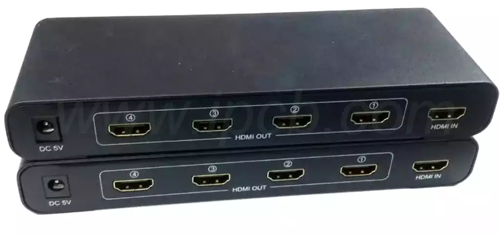
HDMI splitter is a way to HDMI signal into more than two-way function of the device, and split the signal and the source signal is the same, can be synchronized in real time.
In layman’s terms, it is an HDMI interface to expand into multiple HDMI interfaces, so that you can use a host at the same time in multiple monitors show the same picture and sound, like we often go to see the home appliance stores, see a lot of different sizes of TVs support HDMI are playing the same picture, is the use of the HDMI splitter effect!
HDMI, the full name of the English language is High Definition Multimedia Interface, the Chinese name is an acronym for High Definition Multimedia Interface. HDMI not only meets the current highest quality 1080P resolution, but also support for DVD Audio and other state-of-the-art digital audio formats, support for eight-channel 96kHz or stereo digital audio transmission, 192kHz. 192kHz digital audio transmission, and only one HDMI cable connection, eliminating the need for digital audio wiring. At the same time, the HDMI standard has the extra space to be used in future upgrades of audio and video formats.
How HDMI splitter works
HDMI distributor’s work is very simple, that is, 1-way audio and video signals through the chip non-destructive real-time copy into multiple audio and video signals and output, the copying process is similar to our computers to copy the file, the difference is that the HDMI distributor is synchronized in real time, so that we can see the synchronization of the video screen and synchronized audio on multiple monitors.
HDMI interface PCB layout requirements
(1) HDMI interface in accordance with the requirements of the shape of the structure placed on the PCB board edge, easy to plug;
(2) ESD electrostatic protection devices near the HDMI seat placed in the layout, ESD devices must be placed close to the terminals of the HDMI to ensure that the role of ESD can be played out, prioritized over the string of resistance and capacitance;
(3) Others, such as anti-backup circuits, voltage divider circuits, etc. can take the principle of proximity placed near the HDMI seat;
(4) HDMI interface 5V power supply circuit near the HDMI seat placed;
HDMI splitter interface PCB design
- Component layout should be compact, electronic component location should be in accordance with the signal flow direction of the layout, follow the principle of first protection after filtering, ESD protection devices near connect, followed by common mode inductance;
- Each group of differential signal alignment to ensure that the parallel length of the alignment, around the land line package ground, and played a hole to the lower ground; try to avoid changing layers, different layers of impedance and over the hole and other differences will reduce the effect of differential-mode transmission and the introduction of common-mode noise; to avoid resistance discontinuity caused by the 90-degree alignment, can be used as a substitute for arcs or 135-degree folded line.
- In the PCB copper laying design, pay attention to the protection devices and common mode inductance is below the hollowing treatment.
Note:When the HDMI splitter connector works at 28Gbps, please follow the following connector optimization recommendations.
- In the connector alignment to center out. If the high-speed signal in the connector has an end signal does not have a PIN adjacent to the GND, the design should be added next to its GND hole.
- If the interface signal operating rate ≥ 8Gbps, then these interface connectors should be able to meet the corresponding standard requirements (such as HDMI2.1/DP1.4/PCI-E3.0 protocol standards). Recommended use of these manufacturers of connectors: Molex, Amphenol, HRS and so on.
- According to the interface to choose to hollow out a layer or two layers of the ground plane, if hollowing out the connector pad directly below the L2 ground reference layer, the need for compartmentalized reference, that is, the L3 layer to be used as a ground reference layer; if hollowing out the L2 and L3 ground reference layer, then the L4 layer needs to be the ground plane, as a compartmentalized reference layer. Dredging size should be combined with the connector type and determined by simulation according to the actual stacked layer.
- It is recommended that each ground pad in the connector to play 2 ground through-hole, and the ground hole should be as close as possible to the pad.
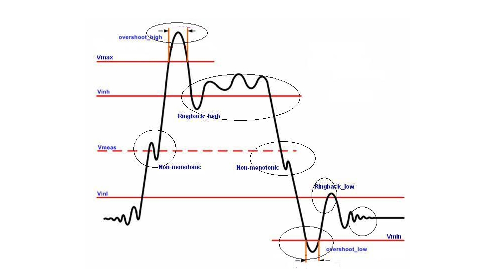
HDMI interface PCB design manufacturability checks
- Impedance line
In the manufacturing process, the tolerance of the impedance line is +/-10%, the general alignment is generally +/-20%, the impedance line is required to be more accurate, so the impedance line design is preferably greater than the general line of the smallest made of capacity. - Soldermask window
HDMI has patch pins, there are plug-in pins, check the HDMI device should pay attention to the pins can not miss the window, and then is the patch pins of the solder resist bridge, open the window of the solder resist bridge needs to be greater than 4mil, otherwise the pins of the different networks are prone to even tin short circuit. - Pin hole
HDMI plug-in pinhole must pay attention to the pin slot hole often leaks the pinhole problem occurs, leaks the pinhole is generally in the turn of the production file, the pin slot hole in the other layer leads to leakage of the turn of the pin slot hole, resulting in a lack of pinhole can not be plugged in.
HDMI splitter with its efficient synchronization and high-definition transmission capabilities, combined with well-designed PCB layout, provides a stable and reliable solution for multi-screen display, leading the new trend of digital audiovisual.