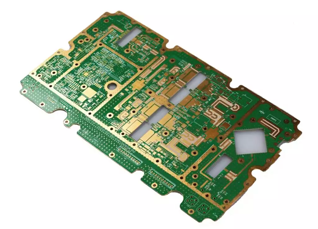
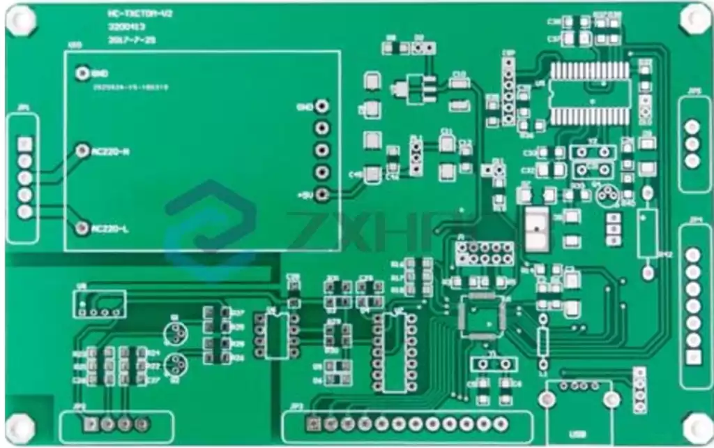
PCB samples refer to the first trial circuit boards produced prior to mass production to validate circuit design and functionality. These samples are typically fabricated by design engineers or manufacturers based on design documentation such as Gerber files and BOMs. PCB samples are commonly used to verify whether the design meets expectations, functions correctly, and whether the manufacturing process is reliable.
The Role of PCB Samples
Verifying Design Feasibility
Producing PCB samples is a crucial step in ensuring designs can be successfully implemented in actual production. Designers use samples to validate critical aspects like circuit layout, component placement, electrical performance, and signal integrity. Only through thorough testing can designers ensure designs won’t encounter serious issues when actually put into production.
Minimizing Production Risks
PCB samples effectively identify potential design flaws, preventing irreparable errors during mass production. Through sample testing, manufacturers can detect design defects and make timely corrections, avoiding costly rework and quality issues that may arise in bulk production.
Optimizing Manufacturing Processes
During sample fabrication and testing, manufacturers not only validate the design itself but also assess the suitability of production processes. For instance, processes like soldering, surface finishing, and component placement are tested during sample production, ensuring smooth execution during mass production.
Accelerating Time-to-Market
By obtaining PCB samples promptly, design teams can rapidly assess whether designs meet requirements and make adjustments in the shortest possible time. This gains valuable time for product R&D progress and time-to-market, while also helping to shorten the product development cycle.
The process of creating PCB samples typically involves the following steps:
Design File Preparation
Before sample production, designers must prepare complete design files, including circuit schematics, PCB layout diagrams (Gerber files), and BOM (Bill of Materials) lists. The quality of these design files directly impacts the sample’s manufacturing quality.
Sample Fabrication and Processing
Based on the design files, PCB manufacturers process the circuit boards. First, they use printing, photolithography, etching, drilling, and other techniques to form the intended traces and pads on the board. Then, components are mounted onto the board according to the BOM, completing the initial PCB sample.
Sample Testing and Validation
After sample completion, engineers conduct electrical performance tests to verify circuit functionality, component placement accuracy, and signal transmission stability. Common tests include functional testing, reliability testing, and thermal testing. These confirm whether the design meets expected requirements.
Modification and Optimization
If issues are identified during testing, the design team optimizes the circuit design or manufacturing process based on test results. Sample modifications typically require iterative cycles until both design and manufacturing processes meet the desired standards.
Importance of PCB Samples
Design Validation
PCB samples are a critical step in design validation. Only through sample verification can designers confirm the rationality and feasibility of their designs. Sample testing provides direct feedback on both circuit functionality and signal integrity.
Cost Control
Without sample testing, design flaws may only surface during mass production, incurring substantial repair and downtime costs. Producing samples early for comprehensive testing effectively minimizes economic losses from design errors.
Accelerating Time-to-Market
For many electronics companies, shortening product development cycles is crucial for enhancing market competitiveness. Rapid PCB sample fabrication and testing significantly reduce time-to-market, accelerating the entire R&D process.
As a critical component in the electronic design workflow, PCB samples not only validate design feasibility but also serve as the bridge connecting concept to mass production. Through rigorous manufacturing processes and multidimensional testing, they enable engineers to identify potential issues early, optimize production techniques, and ultimately achieve cost control and efficiency gains.