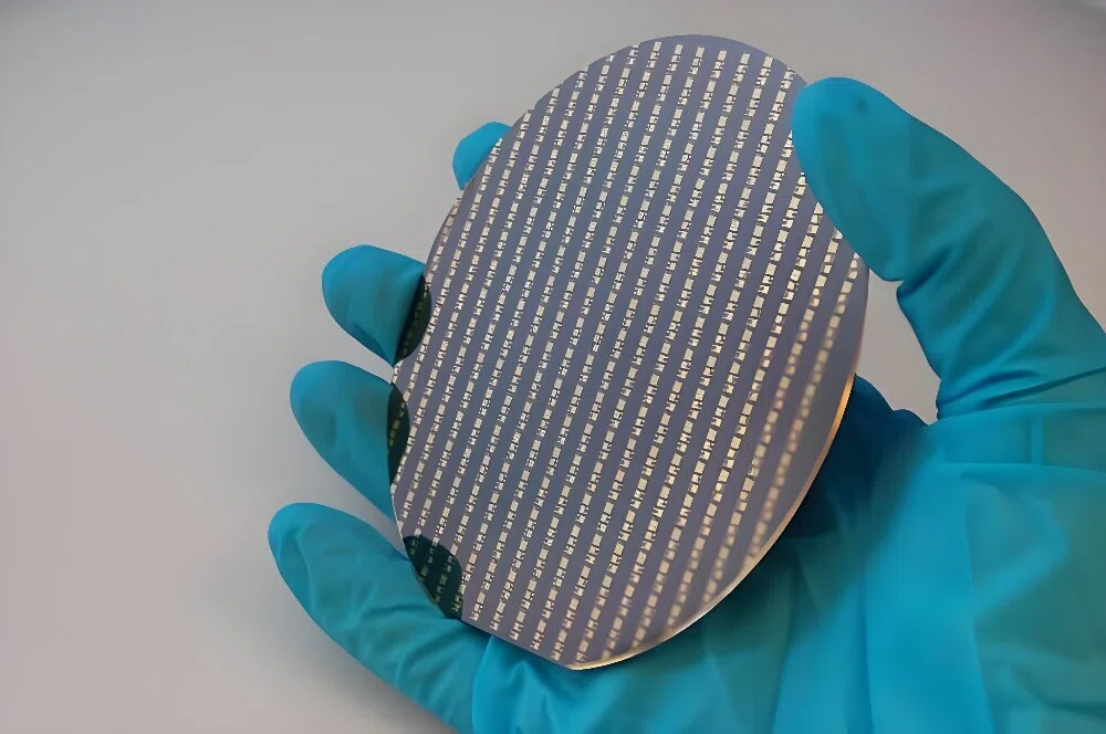
Thick film ceramic pcb is printed metal wiring layer by screen printing process, and then degreased and sintered (generally 850~900℃) to form a circuit. Depending on the viscosity of the metal paste and screen mesh size, the thickness of the prepared metal wiring layer is generally 10μm to 20μm (increasing the thickness of the metal layer can be realized through multiple screen printing).
Power thick film and thin film are materials used in the manufacture of circuit boards. They are an important part of electronic products. Since circuit boards carry many electronic components, the selection of materials and manufacturing processes play a vital role in the performance and stability of the product.
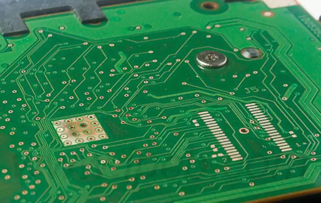
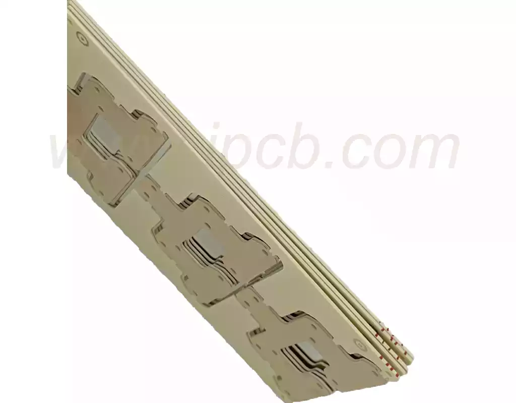
Power thick film and thin film both belong to a kind of copper cladding material. A copper-clad board is a circuit board made by covering electrolyzed copper foil with an insulating material called a substrate, and then chemically or mechanically removing the excess copper foil, leaving the desired pattern of copper foil.
Thick film ceramic substrate features:
- Strong mechanical stress, shape stability; high strength, high thermal conductivity, high insulation; strong bonding, anti-corrosion.
- Better thermal cycling performance, cycle times up to 50,000 times, high reliability.
- With PCB board (or IMS substrate) as can be etched out of a variety of graphic structures; pollution-free, non-polluting.
- Wide operating temperature -55℃~850℃; coefficient of thermal expansion close to silicon, simplifying the production process of power modules.
- Thick film technology involves the addition of a conductor layer (copper or silver) to the ceramic substrate through the screen printing process.
- Suitable for use with aluminum with 2O3/AlN and sapphire substrates.
- A cost-effective solution with fewer manufacturing processes than other methods.
- Conductor thicknesses between 7-20um are less suitable for power electronic devices requiring high current capacity.
- Due to the conductor application,it is also not suitable for designs that require fine tracks and/or plated/filled vias.
Therefore thick film printed ceramic pcb is only used for packaging of electronic devices that do not require high line accuracy, such as automotive electronics.
What are the components that make up a thick film substrate?
Thick film substrates consist of two main types of materials: 1) an insulating substrate material and 2) a thick film paste that is screen printed and fired onto the substrate. In addition, some fired conductors can be used to etch fine line circuits. For example, CMS Circuit Solutions, Inc. typically etches 1 mil lines and 1 mil spacing to maximize circuit density.
Substrate Materials
Typically, thick film materials are applied to ceramic pcb such as aluminum oxide, beryllium oxide (BeO), and aluminum nitride (AlN). The ceramic substrate is the substrate on which the different layers of circuitry are applied. Depending on the requirements of the application, ceramic substrates can also be replaced with different types of materials (i.e. ferrite, sapphire, fused silica, etc.).
Thick Film Pastes
Thick film pastes are divided into three main categories: conductors, dielectrics and resistors. Each paste has two main components:the carrier (organic solvent and plasticizer) and the functional element of the paste (metal, alloy, oxide, or ceramic glass compound). Each thick film slurry is designed for certain properties of the metal, alloy, oxide and/or ceramic glass compound, optimizing their properties based on the application scenario and assembly technique.
Thin-film ceramic substrates utilize thin-film processes such as magnetron sputtering, vacuum evaporation, and electrochemical deposition to form a metal layer on the surface of the ceramic substrate, followed by processes such as masking and etching to form a specific metal pattern.
Features:
Low working temperature, the operating temperature of the whole process is lower than 300℃, which will not cause material and function damage due to high temperature;
High bonding strength between metal-ceramics (>2kg/mm²);
Excellent thermal conductivity, with a thermal conductivity of 24~170W/m-K.
Small thickness of the metal layer on the surface of the TFC substrate (generally less than 1μm) due to the low deposition speed of the sputtering coating;
High wiring precision, the use of mask, etching and other precision operations, can be prepared with high graphic accuracy (line width / line spacing less than 10μm) ceramic substrate;
Controllable thickness of the metal layer.
Thin film ceramic substrate commonly used ceramic substrates: alumina, aluminum nitride and beryllium oxide, etc.; main applications: high power, small size, high heat dissipation requirements, wiring precision requirements of high device packaging. For example, for lasers, LIDAR, LED and other high-power chip packaging.
Differences:
(1) The difference between the film thickness
Thick film ceramic substrate film thickness is generally greater than 10μm, the film thickness of the film is less than 10μm, mostly in less than 1μm;
(2) The difference between the manufacturing process
Thick-film ceramic substrates generally use screen printing process, thin-film ceramic substrates using vacuum evaporation, magnetron sputtering and other process methods.
Thick film ceramic pcb and thin-film ceramic substrates as a key material in circuit board manufacturing, each showing unique performance advantages and application potential. Both together promote the innovation of circuit board manufacturing technology, for the performance of electronic products to improve and diversify the development of a solid foundation.