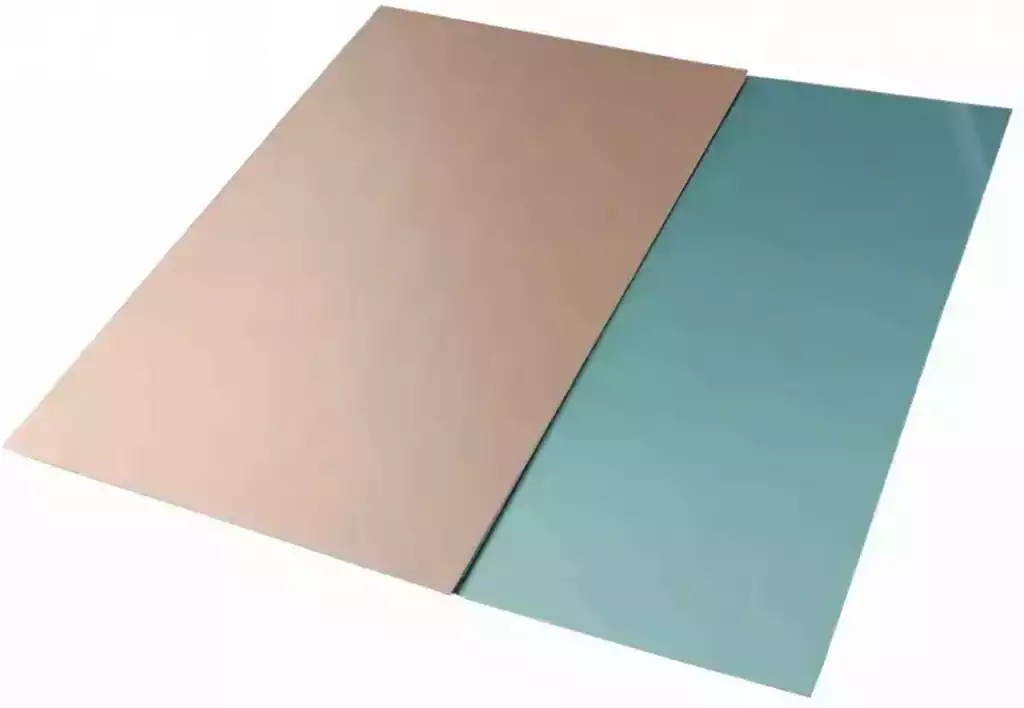
In PCB (Printed Circuit Board) manufacturing, an ounce (OZ) is essentially a unit of weight, which converts to grams (g) roughly as follows: 1 OZ equals approximately 28.35 g. The term 1 OZ refers specifically to the thickness of 1 OZ of copper uniformly covered over an area of 1 square foot (FT2).
The term 1OZ refers specifically to the thickness of copper weighing 1OZ uniformly over an area of 1 square foot (FT2). This is a method of characterizing the average thickness of copper foil by weight per unit area, and is mathematically expressed as 1OZ = 28.35g/ FT2.
Further, we can convert this to length or thickness as follows:
First, we need to know the density constant of copper and the associated unit conversion formula:
The density ρ of copper is 8.9g/cm³
1 centimeter (cm) is equal to 10 millimeters (mm), 1 millimeter (mm) is equal to 1000 microns (um)
1mil is approximately equal to 25.4um
1 FT2 is approximately equal to 929.0304 cm²
Using the mass formula m = ρ x V (volume) = ρ x S (area) x t (thickness), we can derive the thickness of the copper foil: the weight of the copper foil divided by the density of the copper and the area covered gives the thickness of the copper foil.
Based on the previous information, we have 1OZ=t×929.0304cm²×8.9g/ cm³=28.35g/ FT2 (note that FT2 here should be converted to cm² for the calculation, but it is not adjusted here in order to maintain the original formulation).
Therefore, t = 28.35 ÷ 929.0304 ÷ 8.9cm ≈ 0.0034287cm = 34.287um ≈ 34.287 ÷ 25.4mil ≈ 1.35mil.
In summary, the thickness of 1OZ copper foil is approximately 35um or 1.35 mil. similarly, we can derive the following correspondence:
Copper thickness 1OZ (about 0.035mm)
Copper thickness 1.5OZ (about 0.05mm)
Copper thickness 2OZ (approx. 0.07mm)
Factors affecting copper foil thickness
- Signal transmission: The transmission characteristics of circuit boards can be improved by adjusting the thickness of the copper foil, in which the transmission characteristics of the inner layer of the board are more complex than those of the surface layer, and therefore require more precise design.
- Mechanical strength: Setting the right thickness of copper foil can improve the mechanical strength of circuit boards, preventing deformation and damage during manufacture and use.
- Manufacturing process: The thickness of copper foil has a great influence on the production process of circuit boards. Choosing the right thickness of copper foil can help to improve the manufacturing efficiency of the circuit boards and reduce the production cost.
PCB copper foil thickness setting rules
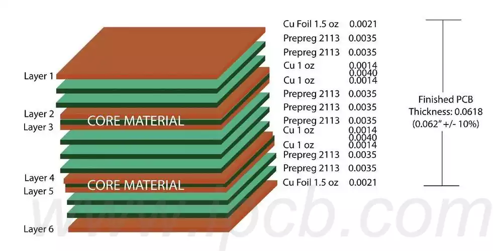
1) Standard thickness range: Common copper foil thicknesses include 1 oz (~35 μm), 2 oz (~70 μm), etc. Special applications can be customised with thicker or thinner copper foils. The selection of copper foil thickness should be based on the current density of the circuit, signal integrity requirements and cost budget.
2) Design specification: During the design phase, engineers need to calculate the minimum copper foil area or width based on the current requirements of the circuit, and then extrapolate the required copper foil thickness. For High Density Interconnect (HDI) boards or high frequency circuits, thinner copper foils may be required to minimise parasitic effects.
3) Manufacturing constraints: The process capability of different PCB manufacturers varies, and the thickness of copper foil for some complex multilayer boards or special requirements may be limited by the manufacturer’s processing capability. Design should be communicated with the manufacturer to confirm in advance.
4) Environmental factors: For PCBs in extreme operating environments (e.g. high temperature, high humidity or high vibration environments), it may be necessary to adjust the thickness of the copper foil to enhance the stability and durability of the circuit.
