Unveiling the Microscopic Geometry and Interconnect Physics of Flip Chips
Traditional wire bonding uses gold or copper wires to connect the electrodes on the front of the chip to the pins of an external substrate via curved leads. This structure is microscopically a one-dimensional periphery arrangement, severely limiting I/O density, and the towering metal arcs introduce significant parasitic inductance, becoming a fatal obstacle to high-frequency electromagnetic wave transmission. Flip chip mounting, on the other hand, “flips” the chip so that its active face directly faces the substrate. Through microscopic metal bumps pre-fabricated on the chip pads, direct electrical and mechanical interconnection is achieved between the chip and the substrate pads on the lower surface, forming a one-to-one area array.
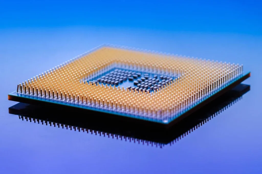
Bump Metallurgy: The Evolution from SnPb to Copper Pillars. Bumps are the core bridge of flip chip interconnects. Its microstructure has undergone dramatic restructuring through generations of materials science: Eutectic SnPb Bumps: The most classic choice for early flip chips. Utilizing the good fluidity of lead (Pb) at eutectic temperatures, the bumps spontaneously melt and collapse during reflow soldering, forming perfectly spherical solder joints. However, under the global trend of lead-free (RoHS) environmental protection, lead has been completely banned. Lead-free SAC Bumps: Using tin-silver-copper alloys (SAC305, etc.) to replace lead. Its melting point soars to over 217°C, and its hardness is higher.
However, under high frequency and high current, severe electromigration easily occurs inside tin-silver-copper bumps—electron storms physically drive metal atoms to migrate, leaving microscopic voids on one side of the bump and forming metal accumulation on the other, ultimately leading to circuit breakage. Copper Pillar Bumps: The ultimate choice for modern ultra-high density flip chips. It directly electroplates a micrometer-thick pure copper cylinder (with exceptionally high conductivity and anti-electromigration properties) onto the chip pads, with only a thin layer of lead-free solder plated at the very tip (Cap). During reflow soldering, the central copper cylinder acts as a “non-melting rigid support,” while only the solder at the tip undergoes molten eutectic bonding. This structure drastically reduces the interconnect pitch from 150 micrometers for traditional solder balls to less than 30 micrometers, achieving an astonishing I/O volume ratio.
The microscopic protective shield of the wafer-level metallization layer (UBM, Under Bump Metallurgy) between the chip’s aluminum (Al) or copper (Cu) pads and metal bumps absolutely cannot be directly soldered. This is because molten solder would aggressively erode (leeaching) the underlying metal, and the lattice mismatch between the two would be severe. Therefore, several layers of special metal thin films, only nanometers thick, must be deposited or sputtered in situ beneath the bumps; this is called UBM (Under Bump Metallurgy). A typical UBM employs a sandwich composite architecture: An adhesion layer (such as titanium (Ti) or chromium (Cr)) firmly adheres to the chip’s native silicon dioxide dielectric layer and aluminum pads.
A barrier layer (such as nickel (Ni) or nickel-vanadium (NiV) acts as a physical barrier, preventing molten solder atoms from capillary diffusion into the chip during soldering, thus protecting the delicate semiconductor PN junction. A wetting layer (such as copper (Cu) or gold (Au) provides perfect surface energy, attracting molten solder to spread rapidly, ensuring high-quality metallurgical cross-linking at the interconnect interface.
Alignment, Eutectic Bonding, and Thermal Stress Relief
The flip chip mounting process is a dynamic process that pushes optical alignment precision, heat conduction, and physical reconstruction to their limits within seconds.
Optical Precision Alignment and Coplanarity Control in Flip Chip Bonders In the mounting stage, the first major challenge faced by flip chip bonders is “blind alignment.” After the chip is flipped, the microbumps on its bottom are completely invisible to the lens above. To achieve micron-level precision alignment, the machine must incorporate a high-resolution prism alignment system (Split-Optics System) with bidirectional lenses. The lenses simultaneously capture images of the chip’s bottom bumps and the substrate’s top pads, and algorithms perform multiple geometric overlap calibrations on these two images in digital space.
When the alignment deviation is corrected to less than 2 micrometers, a high-precision servo spindle presses the chip vertically downwards with extremely smooth pressure. At this point, the placement head must maintain absolute coplanarity. If the chip tilts even by 1 micrometer during pressing, one side of the bumps will experience excessive mechanical pressure, leading to deformation and short-circuiting (solder bridging), while the other side’s bumps will experience non-wet open due to suspension, resulting in a devastating open circuit.
After physical mounting is completed using temperature-controlled profiles for eutectic reflow and transient liquid phase diffusion (TLPD), the component must undergo rapid thermal fusion. Depending on the process, there are two main temperature control methods: Thermocompression Bonding (TCB): The chip mounter has a built-in heater. The moment the chip is pressed against the substrate, the mounter heats up to over 260°C at a rate of several hundred degrees per second, maintaining this temperature for 1 to 2 seconds to instantly melt the solder and then cool and solidify. This method is designed for ultra-thin, highly deformable, ultra-dense chips, but the equipment throughput is extremely low.
Mass Reflow: The chip is temporarily adhered to the substrate using flux, and the entire board is sent into a multi-temperature zone nitrogen-filled reflow oven. Inside the oven, the component undergoes a gentle heating zone, an activation zone, a eutectic zone (above the liquidus line 217°C), and a rapid cooling zone. At the eutectic temperature, inorganic tin and nickel/copper atoms in the UBM undergo intense atomic diffusion at the interface, growing intermetallic compounds (IMCs, such as Ni3Sn4) in situ.
The growth of the IMC layer is thermodynamically necessary (without it, electrical connections cannot be formed), but its physical nature is that of an extremely brittle intermetallic compound. If the reflow time is too long or the temperature is too high, the IMC layer will grow excessively thick (exceeding 3 micrometers), causing the solder joints to undergo catastrophic brittle fracture along the IMC grain boundaries when subjected to subsequent vibrations, much like glass.
The Guardian of Flip Chips
The Rheology and Packaging Reliability of Underfill. After flip chip reflow soldering is complete, the entire interconnect remains in an extremely fragile mechanically exposed state. The linear coefficient of thermal expansion (CTE) of silicon chips is only 3 ppmC, while the CTE of the underlying organic composite substrate (such as a BT substrate) is as high as 15 ppmC. When the chip is powered on and heats up, or when the system undergoes high and low temperature cycling, due to the inherent asymmetry in the expansion rates of the chip and the substrate, the outermost microbumps will be subjected to terrifying shear stress, causing the solder joints to rapidly fatigue tear. To eliminate this mechanical flaw, underfill is indispensable.
Capillary underfill (CUF) is the rheologically limiter of post-fill technology, the most widely used in industry. The process appears simple: a long strip of high-viscosity epoxy resin is sprayed onto the substrate surface on one side of the chip using a high-precision piezoelectric dispensing valve. Upon contact with the chip edge, this resin fluid spontaneously utilizes the microscopic gaps at the chip’s bottom, relying on capillary force, much like water penetrating a sponge, to spontaneously penetrate and fill the space directly beneath the chip, completely filling all spaces and solder ball gaps.
To perfectly achieve this rheological process within a few seconds, the physical parameters of the underfill material must be precisely tuned: ultra-low viscosity and high wettability ensure the resin can spontaneously overcome the flow resistance of 20-micron-level gaps. Nanoscale inorganic ceramic fillers (Silica Fillers): The resin matrix must be forcibly filled with nanoscale silica particles, accounting for over 60% of the volume. These rigid fillers, after curing, forcefully lower the macroscopic CTE of the entire underfill layer from the original 60 ppmC to around 20 ppmC, perfectly matching the silicon wafer and substrate, thus completely eliminating thermal expansion and contraction stress.
However, the introduction of nanoparticles brings another physical nightmare—settling and filtration. When the resin fluid permeates through the extremely dense array of copper pillar bumps, the narrow channels act like filters, forcibly intercepting the silica nanoparticles at the inlet. This causes the fluid to become pure resin (without particle filling) by the time it reaches the middle of the chip. This directly leads to uneven distribution of the coefficient of thermal expansion at the bottom of the chip (lower at the edges, higher in the center), resulting in catastrophic cracking and delamination inside the chip during subsequent thermal shocks.
Therefore, advanced packaging manufacturers must strictly control the D99 particle size of the filler particles (the maximum particle size must be less than 1/3 of the bump pitch) and precisely preheat the substrate (typically 80°C to 110°C) to reduce the dynamic shear viscosity of the resin, enabling unimpeded rheological transport of nanoparticles.
Flip Chip Agile Manufacturing and NPI Supply Chain Strategy
As the global demand for high-performance computing chips, smart wearable systems, and automotive-grade sensors intensifies, flip chip mounting has evolved from an early luxury specialty process into a general-purpose cornerstone of modern advanced packaging. However, flip chip manufacturing has long faced significant technical and lead time barriers due to the high-precision wafer-level dicing, micron-level alignment and mounting, thermoforming furnaces, and high-reliability underfill curing.
The “high walls and aloofness” of traditional advanced packaging giants and the “tape-out hell” of their innovation teams: In the current semiconductor packaging landscape, factories possessing complete wafer thinning, dicing, high-precision flip-chip mounting, and underfill dispensing and curing lines are almost entirely long-established, globally monopolistic OSAT (Outsourced Semiconductor Testing and Assembly) super-large companies. These giants have extremely complex design rules and highly rigid production scheduling mechanisms, exhibiting significant supply chain obstacles when facing rapidly changing market demands for agile innovation and pilot-scale revisions: because a single packaging line at these large companies processes hundreds of thousands of chips per hour, they typically do not accept any small-scale engineering verification samples to amortize equipment depreciation and reel furnace setup costs. Their business entry barriers usually include extremely high new equipment cost (NRE) and minimum order quantity (MOQ) starting at tens of thousands of units.
When university research institutions, agile chip startups, or automotive Tier-1 R&D managers urgently need to prototype and package dozens or hundreds of ASIC bare dies for initial tape-out to test functionality and temperature rise performance, they often face lengthy waiting periods, with delivery times frequently delayed by two to three months or more. In the life-or-death race of semiconductor chips, where “delivery time is life, and being one day earlier in tape-out means seizing market share,” such long packaging and testing lead times can easily disrupt the entire project team’s R&D rhythm, causing R&D funds to be wasted during the prolonged wait.
A truly agile flip-chip packaging and testing service hub with chip-level precision has broken the time constraints of high-density advanced packaging in the R&D prototyping and small-batch stages globally. Leading process integrators have deeply integrated chip-level precision multilayer PCB fabrication, bare die thinning and dicing processes, and 100% agile and flexible advanced packaging pipelines, opening them up to every hardware manager worldwide facing wafer assembly and extreme thermal challenges: True Zero MOQ (Minimum Order Quantity): Whether it’s ultra-dense copper pillar flip-chips with a pitch of less than 40 microns or ceramic multi-chip modules (MCMs) with integrated precision underfill, there are absolutely no minimum order quantity restrictions in the early stages of NPI (New Product Introduction).
Even if you only need to urgently package 5 or 10 bare chips for R&D verification, the advanced application engineering team will instantly initiate a 1-on-1 expert-level flip-chip manufacturability (DFM/DFP) process pre-review, completely avoiding eutectic solder joint failures caused by pad warpage or incorrect UBM selection. Lightning-fast Advanced Packaging and Testing Delivery Time: The factory maintains a constant supply of high-quality, automotive-grade specialty underfill adhesives and matching precision stencils, among other packaging and testing accessories. Utilizing a dedicated flexible flip-chip prototyping line, it completely shatters the months-long delivery time of traditional packaging and testing giants, directly compressing the turnaround time from bare die to finished flip-chip devices to within 7 to 10 days.
Impeccable, High-Reliability Packaging and Testing White Paper: Every delivered flip-chip device undergoes extremely rigorous physical testing before leaving the factory. Each order comes standard with a comprehensive third-party authoritative quality report, including 100% ultrasonic scanning microscopy (C-SAM) non-destructive testing drawings (to prove that the bottom filler layer is 100% filled and free of any micro-bubbles or particle sedimentation/delamination defects), high-magnification X-ray 3D inspection images of bent pins and micro-bump misalignment, and metallographic microsection analysis to prove that the IMC intermetallic compound thickness is perfectly within the golden range of 1 to 3 micrometers. Advanced packaging and testing data ensures that every interconnect pin exhibits steel-like conductivity and heat dissipation stability under extreme high-frequency operation.