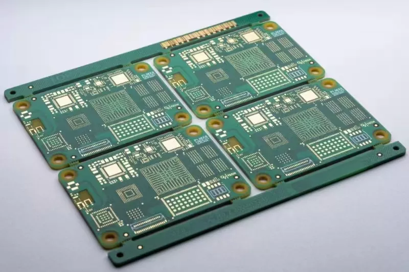
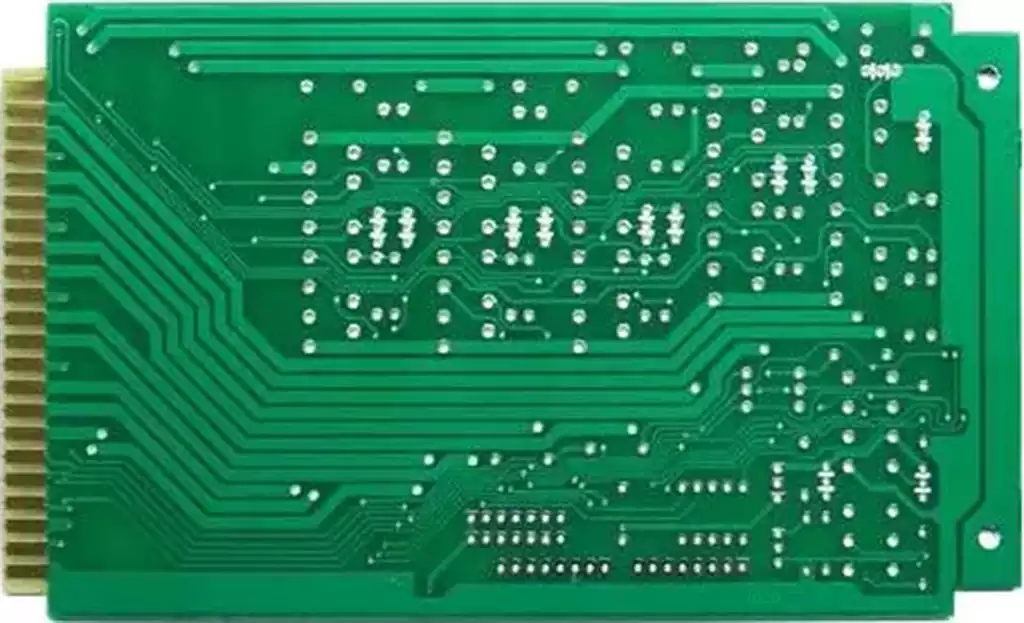
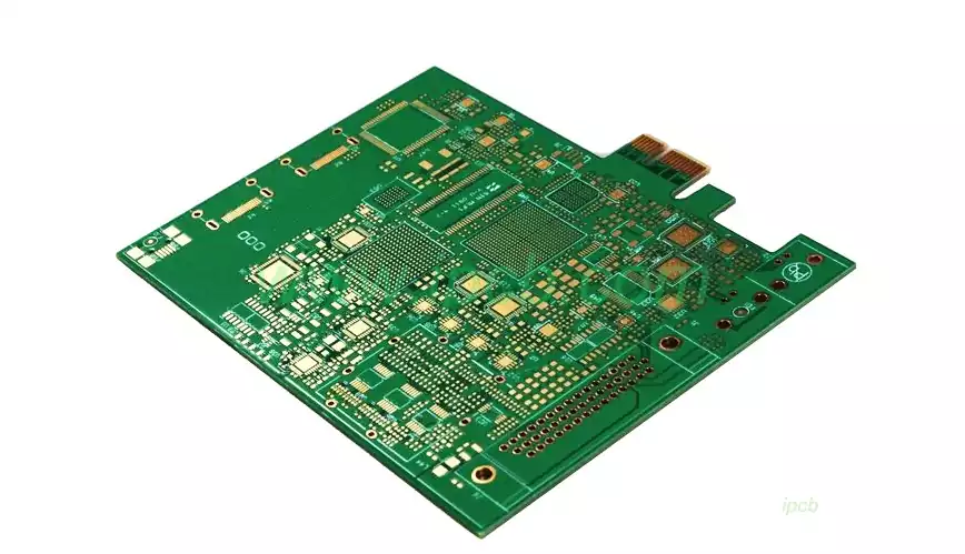
What is a circuit board? It is also called printed circuit board and is one of the important components of the electronics industry. It is an electronic component used to support and electrically connect electronic components. Almost every electronic device, from small electronic watches and calculators to large computers, communication electronics, and military weapons systems, uses printed circuit boards for electrical interconnections between electronic components such as integrated circuits.
The most essential success factor in the research process for larger electronic products is the design, documentation, and manufacture of the printed circuit board for that product. The quality of the design and manufacture of the printed circuit board has a direct impact on the quality and cost of the overall product, and can even lead to the success or failure of the business competition.
PCB fabrication steps
Step 1: Design and Output
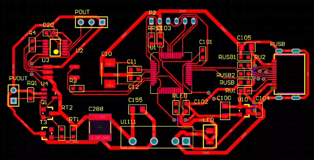
The circuit board should be strictly compatible with the PCB layout created by the designer using PCB design software. Commonly used PCB design software includes Altium Designer, OrCAD, Pads, KiCad, Eagle, and so on. Note: Prior to PCB fabrication, designers should inform their contract manufacturer about the version of PCB design software used for circuit design, as it helps avoid problems caused by discrepancies.
Once the PCB design is approved for production, the designer can export the design to a format supported by the manufacturer. The most commonly used program is called Extended Gerber. the name of Gerber is also known as IX274X.
The PCB industry has spawned Gerber as the perfect output format extension. Different PCB design software may require the use of different Gerber file generation steps, all of which encode comprehensive and important information, including copper trace layers, drill plans, holes, component symbols, and other options. At this point, all aspects of the PCB design are checked. The software performs supervisory algorithms on the design to ensure that no errors are found. The designer also checks the plan for elements related to alignment width, board edge spacing, alignment and hole spacing, and hole size.
After a thorough check, the designer forwards the PCB file to the PC boardroom for production. To ensure that the design meets the minimum tolerances required for the manufacturing process, almost all PCB Fab Houses perform a Design for Manufacturing (DFM) check before the boards are manufactured.
Step 2: From File to Movie
After the PCB schematic file has been output by the designer and DFM checked by the manufacturer, the PCB printing process begins. The manufacturer uses a special printer called a plotter to make photographic films of the PCB to print the circuit board. The manufacturer will use these films to image the PCB. Although it is a laser printer, it is not a standard laser printer. The plotter uses incredibly precise printing techniques to deliver highly detailed film of the PCB design.
The final product will result in a plastic sheet of PCB negative with black ink. For the inner layer of the PCB, the black ink represents the conductive copper portion of the PCB. The rest of the clear portion of the image represents areas of non-conductive material. The outer layer follows the opposite pattern: the copper layer is cleared, but the black color refers to the area that will be etched away. The plotter automatically develops the film and stores it securely to prevent unwanted contact.
Each layer of the PCB and soldermask has its own transparent black film sheet. A total of four sheets are required for a two-layer PCB: two for the multilayer and two for the soldermask. It is important that all the films must correspond perfectly with each other. When used harmoniously, they map out the PCB alignment.
In order to achieve perfect alignment of all films, positioning holes should be punched in all films. The accuracy of the holes can be achieved by adjusting the table where the films are located. Holes are punched when minor alignment of the table results in the best match. These holes will be fitted with locating pins in the next step of the imaging process.
Step 3: Printing the inner layer: where will the copper flow? The film creation in the previous step was intended to map out a copper line graphic.
Now it’s time to print the graphic from the film onto the copper foil.This step in PCB manufacturing prepares the actual PCB for fabrication.The basic form of a PCB consists of a laminate whose core materials are epoxy resin and fiberglass, also known as the substrate.The laminate is the ideal body to receive the copper that makes up the PCB.The substrate material provides a strong and dustproof starting point for the PCB.The copper is pre-bonded together on both sides.The process involves abrading the copper to reveal the design in the film.Cleanliness is critical in PCB construction.The copper-faced laminate is cleaned and then sent to a decontamination environment.At this stage, it is vital that no dust particles are deposited on the laminate.The wrong kind of dirt can cause circuits to short out or remain disconnected.Next, the cleaned panel receives a photosensitive film layer known as a photoresist.The photoresist includes a layer of photo-reactive chemicals that harden after exposure to UV light.This ensures an exact match from the photographic film to the photoresist.The film is mounted on pins that hold the pins in place on the laminate.The film and cardboard are lined up and receive a beam of ultraviolet light.The light passes through the transparent portion of the film and hardens the photoresist on the copper below.The black ink of the plotter prevents the light from reaching the undesired hardened areas, so it is removed.When the plate is ready, it is washed with an alkaline solution to remove any unhardened photoresist.A final pressure wash will remove anything else left on the surface.The plate will then be dried.The product will emerge with a resist that will properly cover the areas of copper to be retained in its final form.The technician inspects the board to ensure that no errors have occurred at this stage.All of the resist present at this point indicates the copper that will be exposed in the finished PCB.This step only applies to boards with more than two layers.Simple two-layer boards can skip drilling.Multi-layer boards require more steps.
Step 4: Remove Unwanted Copper
After removing the photoresist and covering the copper we want to keep with hardened photoresist, the board will move on to the next stage: removing the unwanted copper.Just as the alkaline solution removes the resist, more powerful chemicals consume the excess copper.A copper solvent solution bath removes all exposed copper.Meanwhile, the desired copper remains fully protected beneath the hardened layer of photoresist.Not all copper boards are created equal.Some heavier boards require large amounts of copper solvent and variable exposure times.As a side note, heavier copper boards require special attention to track spacing.Most standard PCBs rely on similar specifications.Now that the solvent has removed the excess copper, the hardened resist that protects the preferred copper needs to be washed off.Another solvent will accomplish this task.The board is now flashed only with the copper substrate required for the PCB.
Step 5: Layer Alignment and Optical Inspection
With all layers clean and ready to go, the layers need to be aligned with the punch to make sure they are all aligned. Locating holes align the inner layers with the outer layers. The technician places the layers into a machine called an optical punch, which allows for precise correspondence and therefore accurate punching of the locating holes.
Once the layers are placed together, it is impossible to correct any errors that occur on the inner layer. Another machine performs an automatic optical inspection of the panels to confirm that there are no defects at all. The manufacturer receives the original Gerber design as a model. The machine scans the layers using a laser sensor and then electronically compares the digital image to the original Gerber file.
If the machine finds inconsistencies, the comparison is displayed on a monitor for technicians to evaluate. Once the layer passes inspection, it moves on to the final stage of PCB production.
Step 6: Layering and Binding At this stage, the board is molded
All the individual layers wait for their union. After preparing and confirming the layers, they simply need to be fused together.The outer layers must be connected to the substrate.The process is divided into two steps: layering and binding.
The outer ply consists of fiberglass sheets prepreg impregnated with epoxy resin.It is referred to simply as prepreg. Thin copper foils also cover the top and bottom of the original substrate, which contains the copper conductors etched.Now it’s time to clamp them in the center.
Bonding occurs on a heavy-duty steel table with metal clips.The layers are firmly secured in pins attached to the table. Everything must fit tightly to prevent movement during the alignment process.
The technician first places the prepreg layers on the alignment basin.The substrate layer is placed on top of the prepreg before the copper sheet is placed.The other sheets of prepreg are located on top of the copper layer. Finally, the stack is completed with aluminum foil and a copper press.It is now ready for pressing.
The entire procedure is performed automatically by the bonding machine computer. The computer schedules the process of heating the stack, the time to apply pressure and the time to allow the stack to cool at a controlled rate.
Next, a certain amount of unwrapping occurs.During the process of molding all the layers together, the PCB’s shine and the technician simply unpacks the multilayer PCB product. Removing the restraining pins and discarding the top pressure plate is a simple matter. the PCB benignly emerges from its aluminum platen shell.The copper foil included in the process still retains the outer layer of the PCB.
Step 7: Drilling
Finally, holes are drilled in the stacked boards.All of the components scheduled for later introduction, such as copper connections on the through-hole and lead side, rely on the accuracy of precision drilling.Holes are drilled to the width of a hair – the drill bit reaches a diameter of 100um, while the average diameter of a hair is 150um.To locate the drill target, an X-ray locator identifies the appropriate drill target point. Holes are then drilled in the appropriate locator holes to secure the stack for a series of more specific holes.
Prior to drilling, technicians place a plate of cushioning material below the drill target to ensure a clean drill hole is formed.The exit material prevents any unwanted tearing to the exit of the drill bit.
A Computer Controls Every Tiny Movement of the Drill – Products that determine the performance of a machine naturally rely on computers. The computer-driven machine uses the drill file from the original design to recognize the proper drill position.
The drill head uses a pneumatic spindle and spins at 150,000 rpm – at this speed you might think that drilling is instantaneous, but there are a lot of holes to be drilled.An average circuit boards contains over a hundred complete points.Each drill requires its own special moment during the drilling process and therefore takes time. Afterwards, these holes will accommodate the PCB’s over-holes and mechanical mounting holes.The final fixing of these parts takes place after plating.
After the drilling is completed, the additional copper lining the edges of the production panel is removed by means of a profiling tool.
Step 8: Plating and Copper Deposition
After drilling, the panels are moved to plating. This process uses chemical deposition to fuse the different layers together. After thorough cleaning, the panel is subjected to a series of chemical baths. In a fusion bath, the chemical deposition process deposits a thin layer of copper (approximately 1um thick) on the surface of the panel. The copper enters a recently drilled hole.
Prior to this step, the inner surface of the hole exposes only the fiberglass material that makes up the interior of the panel. The copper grooves completely cover or cover the walls of the hole. Incidentally, the entire panel receives the new copper layer. Most importantly, the new hole is covered. A computer controls the entire process of impregnation, removal and processing.
Step 9: Imaging the outer layer
In step 3, we applied photoresist to the panel.In this step, we will perform this operation again – this time with the exception that we image the outer layer of the panel using the PCB design.We first place the layers in a sterile room to prevent any contaminants from adhering to the layer surfaces, and then apply a layer of photoresist to the panel.The prepared panel goes into the yellow room.UV light affects the photoresist. The UV levels at yellow wavelengths are not sufficient to affect the photoresist.
The black ink transparencies are held in place by pins to prevent alignment with the panel.When the panel comes into contact with the stencil, the generator sandblasts it with high-intensity UV light, which hardens the photoresist. The panel then enters a machine that removes the unhardened resist and is protected by black ink opacity.This process is the reverse of the process for the inner layers.Finally, the outer panel is inspected to ensure that all unwanted photoresist was removed in the previous stage.
Step 10: Plating
We return to the plating chamber.As we did in Step 8, we plated a thin layer of copper on the panel.The exposed portion of the panel from the outer photoresist table receives the plated copper.After the initial copper plating bath, the panel is usually tinned, which removes all of the copper that is scheduled to be removed from the panel.The tin protects a portion of the panel so that it remains covered with copper during the next etching stage. Etching removes unwanted copper foil from the panel.
Step 11: Final Etching
At this stage, tin protects the desired copper.Unwanted bare copper and residual copper underneath the resist layer is removed.Again, a chemical solution is applied to remove excess copper.Meanwhile, tin protects the valuable copper at this stage.The conductive areas and connections are now properly established.
Step 12: Solder Resist Film Application
Before applying the soldermask to both sides of the board, the panel is cleaned and covered with epoxy soldermask ink.The board receives a beam of UV light that passes through the soldermask photographic film. The covered portion remains unhardened and will be removed.
Finally, the board goes into an oven to cure the solder resist.
Step 13: Surface Molding
To increase the solderability of the PCB, we chemically plated them with gold or silver. Some PCBs also receive hot air leveling pads during this stage.Hot air leveling produces a uniform pad. This process leads to the creation of surface molding, which can be handled in many types according to specific customer requirements.
Step 14: Screen Printing
The nearly finished board receives inkjet writing on its surface to indicate all the important information related to the PCB, which finally enters the final stage of coating and curing.
Step 15: Electrical Testing
As a final precaution, the technician performs an electrical test on the PCB board. An automated program confirms the functionality of the PCB and its conformance to the original design. At the PCB manufacturer, advanced electrical testing called “flying probe testing” is offered, which relies on moving probes to test the electrical properties of each network on the bare board.
Step 16: Profiling and V-grooving
Now we come to the final step: cutting.Different boards were cut from the original panel.The methods employed focused either on using a routing tool or on using v-grooves. router planers leave small protrusions along the edges of the board, while v-grooves cut diagonal channels along the sides of the board.Both methods allow the board to be easily ejected from the panel.