Copper in PCB, also known as PCB Copper Overlay, is an area of a PCB layer that is filled with copper. The layer can be the top, bottom, or any interior of the PCB stack, and PCB copper cladding can be used as a ground, reference, or to isolate specific components or circuits from the rest of the elements of the layer.
PCB Copper Cladding Methods:
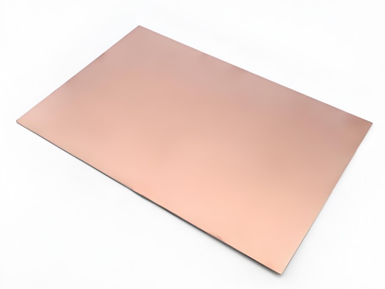
1.Large area copper cladding
Large-area copper cladding has increased the current and shielding double role, but large-area copper cladding, if the wave soldering, the board may be warped, and even blistering. Therefore, large-area copper cladding will generally open a few slots to alleviate copper foil blistering.
2.Grid copper cladding
From the point of view of heat dissipation, it reduces the heat surface of the copper, but also plays a certain role in electromagnetic shielding. Therefore, high-frequency circuits require high anti-jamming copper grid; low-frequency circuits, high-current circuits and other commonly used large-area copper cladding.
The thickness of copper in PCB:
1.General single, double-sided PCB board copper foil (copper cladding) thickness of about 35um (1.4mil).
2.There is another specification for 50um is not common.
3.Multilayer board surface layer is generally 35um (1.4mil), the inner layer of 17.5um (0.7mil).
4.Copper foil thickness is also useful for OZ (ounces) that 1OZ refers to 1OZ of copper uniformly covered in 1 square foot area of copper thickness, that is, about 1.4 mil. This is also the reason that we always feel that the size of those odd.
The role of copper in PCB:
1.Signal transmission enhancement
Circuit board signal transmission quality for circuit board performance and stability are very important. A major role in the PCB copper cladding is to enhance the stability of signal transmission. When the signal transmission from one endpoint to another, the copper layer will form a signal pathway between the two endpoints, so that the signal will be able to pass more stably, thus making the overall signal transmission performance is more outstanding.
2.Reduce noise interference
In electronic equipment, there will be a lot of electromagnetic interference and other noise interference, and copper cladding on the PCB can effectively reduce this interference. Generally, copper cladding will flow at a high frequency without contact on the whole PCB, thus generating an electric field on the whole circuit board, and this electric field can effectively shield noise interference.
3.Heat dissipation
PCB on the operation of electronic components, will produce a lot of heat, if the heat can not be dissipated, will lead to the aging and failure of electronic components. Therefore, heat dissipation is very important. Copper coating on PCB can effectively improve the efficiency of heat dissipation, thus ensuring the normal operation of electronic components.
4.Copper balance
PCB grounding copper cladding can also be achieved during PCB assembly by balancing the amount of copper on both sides of the board to achieve the contract manufacturer (CM), reducing the possibility of warpage during reflow. In this case, grid copper cladding may be a better alternative to solid copper grounding cladding.
5.Increase current carrying capacity
Conductive lines used on PCBs are usually made of copper foil. Compared with other metals, copper has a very high electrical and thermal conductivity, which means it can carry more current. Copper cladding on the PCB can increase the total current carrying capacity of the circuit, thus ensuring that the circuit works properly.
6.Easy PCB manufacturing
Provide a uniform distribution of copper on a layer, making the etching and plating process better and reducing the amount of etching solution used in the PCB manufacturing process (reducing costs).
7.Improve mechanical strength
Copper cladding can effectively improve the mechanical strength of the PCB to avoid PCB bending, wear and tear, cracks, etc. during use. Copper is a very tough metal, can well resist the flexing, tearing, tensile force and other external forces. Therefore, the use of copper cladding can enhance the structural stability of the PCB and improve the service life of the circuit board.
8.Protect the PCB
PCB on the other metal lines and components are very susceptible to oxidation, corrosion and other damaging effects. Copper cladding on the PCB can be used as a layer of protection, can protect other lines and components will not be eroded by natural factors or pollutants. In addition, chemical corrosion and air pollution generated in the PCB manufacturing process can be eliminated by the copper cladding.
Copper in PCB plays a very important role in the PCB, it can enhance signal transmission, reduce noise interference, improve heat dissipation, increase current carrying capacity, improve mechanical strength, protection of the PCB and so on. I believe that in the near future, with the application of new technologies and copper cladding process continues to improve, the role of copper cladding will be further highlighted.