In modern electronic equipment, the design and manufacture of radio frequency (RF) PCBs are receiving more and more attention. With the rapid development of wireless communications and a variety of high-tech products, the coupling of RF PCBs has become one of the most important factors affecting the quality of signal transmission and overall system performance. In this paper, we will discuss in depth what is the RF PCB coupling, the type of coupling, the mechanism and the importance of practical applications and solutions.
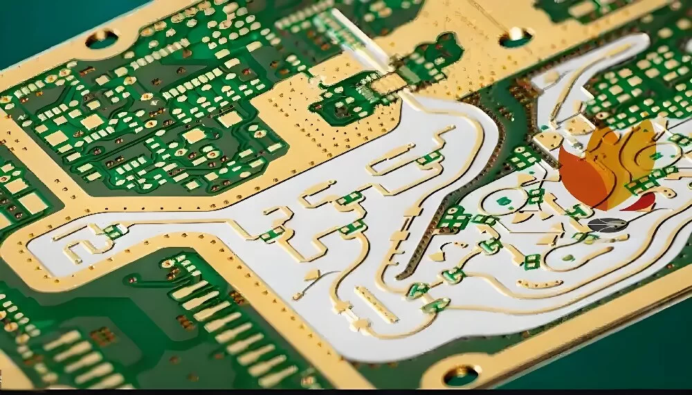
RF PCB overview
RF PCB is a printed circuit board used for high-frequency signal transmission, which is widely used in wireless communications, satellite communications, radar, medical equipment and many other fields. With the continuous development of science and technology, RF technology gradually to higher frequencies and smaller size development, which puts forward higher requirements for the design of RF PCB, designers must ensure the stability and reliability of the signal in a complex electromagnetic environment.
RF signals are usually in the range of several hundred MHz to several GHz, the characteristics of this high-frequency signal make it easy to be affected by various factors in the transmission process, such as electromagnetic interference, signal attenuation and so on. Therefore, in RF PCB design, the coupling problem is particularly important, because it directly affects the signal integrity and system performance.
The definition of coupling
Coupling refers to the process in which a signal source affects another signal source through some mechanism in a circuit. In RF PCB, coupling mainly refers to the interaction between signals, which can be intentional (e.g., signal transmission) or unintentional (e.g., interference). For example, in wireless communications, coupling between the transmitting and receiving signals is desired by the designer, while interference between the two signal sources is to be avoided in undesired situations.
The essence of coupling is the action of electromagnetic fields, which can be realized in different ways, such as electric field coupling, magnetic field coupling and electromagnetic radiation coupling. These coupling methods have their own characteristics in RF PCB design, for designers to understand these coupling mechanisms to help optimize circuit performance, to ensure the accurate transmission of signals.
In the RF PCB, coupling can be divided into the following types:
Electric field coupling Electric field coupling refers to the phenomenon of two conductors interacting with each other through an electric field. In RF PCB, electric field coupling usually occurs between neighboring conductors, especially in high-frequency signal transmission, the electric field of the signal will have an impact on the surrounding conductors, resulting in the coupling phenomenon. This type of coupling may cause signal distortion, and designers need to optimize the layout to minimize this effect.
Magnetic field coupling Magnetic field coupling refers to the way of signal transmission through magnetic fields. In RF PCBs, magnetic field coupling occurs mainly between components such as transformers or inductors. When current passes through a conductor, it generates a magnetic field around it, and this field can affect nearby conductors, leading to signal coupling. Designers need to consider the distance and arrangement between components to minimize unwanted magnetic field coupling.
Radiative coupling Radiative coupling refers to the way in which signals are transmitted through electromagnetic waves. This type of coupling is usually important in the transmission of high frequency signals. When the signals in the RF PCB are propagated, the conductors in the surrounding environment may receive these electromagnetic waves, leading to coupling phenomena. Such coupling in the design needs special attention to ensure signal integrity.
The mechanism of coupling
RF PCB in the coupling mechanism mainly includes the following aspects:
Signal propagation RF signals propagate in the form of electromagnetic waves on the PCB. In the propagation process, the electric and magnetic fields of the signal will interact with the surrounding conductors, resulting in a coupling effect. This coupling effect may lead to distortion or attenuation of the signal, thus affecting the performance of the entire circuit. Therefore, designers need to consider the propagation path of the signal and optimize the circuit design to reduce the negative impact of coupling.
Electromagnetic Interference In RF PCBs, electromagnetic interference is one of the major causes of coupling problems. When there are multiple signal sources in the PCB, electromagnetic interference between them can lead to coupling between signals. Designers need to consider how to minimize EMI to improve the system’s immunity to interference, which usually requires a proper layout of the circuit to avoid high-frequency signal lines crossing each other.
Impedance Matching Impedance matching is an important factor affecting RF PCB coupling. Impedance mismatch can lead to signal reflection and loss, thus affecting the coupling effect. When designing an RF PCB, you need to ensure that the impedance between the signal source, transmission line and load is matched to achieve the best signal transmission effect. The use of appropriate impedance matching network can greatly improve the quality of signal transmission.
Factors affecting coupling
The effect of coupling is affected by a variety of factors, mainly including the following aspects:
Circuit layout Circuit layout is an important factor affecting coupling. Designers need to consider the spacing between the signal lines in the layout, the way of alignment, etc.. A reasonable layout can reduce unnecessary coupling and avoid signal interference. For example, designers can reduce the impact of coupling by increasing the distance between signal lines or by arranging high-frequency signal lines separately from low-frequency signal lines.
Material Selection The selection of PCB materials has a direct impact on the coupling effect. The dielectric constant, conductivity and other parameters of different materials affect the signal propagation characteristics. Therefore, the selection of suitable materials is an important step to optimize the coupling. When selecting materials, designers need to consider the operating frequency, temperature range and environmental factors to ensure that the selected material can meet the design requirements.
Environmental factors Environmental factors such as temperature, humidity and electromagnetic interference can also affect the coupling effect. Designers need to take these external factors into account when designing to improve the stability and reliability of the system. For example, in a high humidity environment, the dielectric constant of the PCB material may change, thus affecting the signal transmission characteristics.
The importance of coupling in practical applications
Coupling plays an important role in the practical application of RF PCB. Good coupling can improve the signal transmission efficiency and system stability, on the contrary, poor coupling can lead to signal distortion, system instability, and even cause equipment failure.
Signal Integrity In RF applications, signal integrity is critical. Good coupling design can ensure the integrity of the signal in the transmission process, to avoid signal distortion caused by poor coupling. This is especially important for high-frequency signals, which have a more significant impact on the time and frequency domains. Therefore, the signal path needs to be carefully analyzed in the design to ensure a clear and stable signal.
Anti-jamming capability In a complex electromagnetic environment, good coupling design can improve the anti-jamming capability of the RF PCB. Through reasonable layout and design, the interference between signals is reduced and the reliability of the system is improved. Designers can use shielding technology, filters and other methods to improve the anti-interference ability to ensure stable signal transmission.
System performance Coupling has a direct impact on the overall performance of the RF system. Optimizing the coupling design can improve the transmission efficiency of the system, reduce energy consumption and achieve higher performance indicators. This is especially important in applications in communications, medical and military fields. Designers need to constantly explore new design methods to improve the performance of RF PCBs.
Coupling design challenges and solutions
In RF PCB design, the challenges of coupling issues mainly include signal interference, design complexity, and manufacturing tolerances. For these challenges, designers can take the following kinds of solutions:
Optimize the layout When designing RF PCBs, the coupling between signals can be effectively reduced by optimizing the layout. Reasonable arrangement of component locations, increase the spacing between signal lines to avoid unnecessary electromagnetic interference. For example, layered wiring techniques can be used to separate the signal lines of different frequency bands in the layout, thus reducing the coupling between each other.
Selection of appropriate materials The use of materials with good high-frequency characteristics can reduce signal loss and improve the coupling effect. Designers should choose appropriate PCB materials according to specific applications to optimize signal transmission. Selecting materials with low dielectric constants and low loss factors can significantly improve the transmission characteristics of high-frequency signals.
Use of Shielding Technology In high interference environments, the use of shielding technology can effectively reduce the impact of external electromagnetic interference on the signal. By introducing a shielding layer in the circuit, the anti-interference capability of the system can be improved to ensure signal stability.
Conclusion
In RF PCB design, the coupling problem is a factor that cannot be ignored. By gaining a deeper understanding of the definition, types, mechanisms and influencing factors of coupling, designers are able to take corresponding measures in practical applications to optimize signal transmission and system performance. With the progress of technology, the study of coupling will continue to be in-depth, providing new ideas and directions for the development of RF PCB.
